Download
1 / 41
640 likes | 1.21k Vues
Chapter 3. PIC18F Programming Model and Its Instruction Set. Data Memory Organization. PIC16F8F2520/4520 Register File Map. 000h. Access RAM. 07Fh. 080h. Bank 0 GPR. 0FFh. 100h. Bank 1 GPR. Data Memory up to 4k bytes Divided into 256 byte banks

E N D
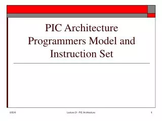
Chapter 3 PIC18F Programming Model and Its Instruction Set
Data Memory Organization PIC16F8F2520/4520 Register File Map 000h Access RAM 07Fh 080h Bank 0 GPR 0FFh 100h Bank 1 GPR • Data Memory up to 4k bytes • Divided into 256 byte banks • Half of bank 0 and half of bank 15 form a virtual bank that is accessible no matter which bank is selected Remember: 1FFh 200h Bank 2 GPR Access Bank 2FFh Access RAM 00h 7Fh Access SFR 80h FFh D00h Bank 13 GPR 256 Bytes DFFh E00h Bank 14 GPR EFFh F00h Bank 15 GPR F7Fh F80h Access SFR FFFh
Register File Concept Data Memory (Register File) • Register File Concept: All of data memory is part of the register file, so any location in data memory may be operated on directly • All peripherals are mapped into data memory as a series of registers • Orthogonal Instruction Set: ALL instructions can operate on ANY data memory location w f 07h ALU 08h 09h 0Ah 0Bh Data Bus d w f 0Ch 0Dh 0Eh 0Fh 10h WREG Decoded Instruction from Program Memory: Opcode d a Address Arithmetic/Logic Function to be Performed Address of Second Source Operand Result Destination
PIC18F Programming Model (1 of 2) • The representation of the internal architecture of a microprocessor, necessary to write assembly language programs • Programming Model • Two Groups of Registers in PIC16 8-bit Programming Model • ALU Arithmetic Logic Unit (ALU) • Special Function Registers (SFRs) from data memory
Registers • WREG • 8-bit Working Register (equivalent to an accumulator) • Used for arithmetic and logic operations • BSR: Bank Select Register (0 to F) • 4-bit Register • Only low-order four bits are used to provide MSB four bits of a12-bit address of data memory.
Register Direct Addressing BSR (Bank Select Register) ‘f’ Operand 12-bit Effective Address (Use this when coding) ‘a’ Bit from Instruction 4-bits from BSR Register 8-bits Encoded in Instruction 0 0 1 0 1 0 0 0 0 0 1 0 0x282 Bank15 Bank0 Bank1 Bank2 Bank13 Bank14 00 FF FF FF FF FF FF 01 FF FF FF FF FF FF 02 FF FF FF FF FF FF 03 FF FF FF FF FF FF 7D FF FF FF FF FF FF 7E FF FF FF FF FF FF 7F FF FF FF FF FF FF 80 FF FF FF FF FF FF 81 FF FF FF FF FF FF 82 FF FF FF FF FF FF FC FF FF FF FF FF FF FD FF FF FF FF FF FF FE FF FF FF FF FF FF FF FF FF FF FF FF FF
Example: 9F+52 =F1 1001 1111 0101 0010 ------------- 1111 0001 N=1,OV=0, Z=0, C=0, DC=1 STATUS: Flag RegisterFlags in Status Register • C (Carry/Borrow Flag): set when an addition generates a carry and a subtraction generates a borrow • DC (Digit Carry Flag): also called Half Carry flag; set when carry generated from Bit3 to Bit4 in an arithmetic operation • Used for BCD representation • Z (Zero Flag): set when result of an operation is zero • OV (Overflow Flag): set when result of an operation of signed numbers goes beyond seven bits • N (Negative Flag): set when bit B7 is one of the result of an arithmetic /logic operation
File Select Registers (FSR) (1 of 2) • Three registers holding 12-bit address of data registers • FSR0, FSR1, and FSR2 • File Select Registers composed of two 8-bit registers (FSRH and FSRL) • Used as pointers for data registers for indirect addressing • Associated with index (INDF) registers Find FSR0-FSR2 in Special Function Register – page 64 What are the File addresses for each? / How many INDF do you find?
Program Counter 21-bit register functions as a pointer to program memory during program execution • 21-bit PC can access up to 221 = 2MB (1MWord) • 22nd bit used to access configuration memory at program time or via table reads & writes • Contains address of NEXT instruction (pipelining) • Lower byte accessible in data memory as PCL • Upper bytes indirectly accessible via PCLATH/PCLATU • Bit 0 of PC is always ‘0’ except when reading or writing program memory via table read/write mechanism PCU PCH PCL 21 20 19 18 17 16 15 14 13 12 11 10 9 8 7 6 5 4 3 2 1 0 0 0 0 0 0 0 0 0 0 0 0 0 0 0 0 0 0 0 0 0 0 0 Program Counter
Program Memory is Byte Addressable • Low byte has even address, high byte has odd address • Addresses of instructions are always even Word Address 16-bit Program Memory High Byte Address Low Byte Address 0 0 0 0 0 0 0 0 0 0 0 0 0 0 0 0 0x000001 0x000000 0 0 0 0 0 0 0 0 0 0 0 0 0 0 0 0 PC 0x000003 0x000002 0 0 0 0 0 0 0 0 0 0 0 0 0 0 0 0 0x000005 0x000004 0 0 0 0 0 0 0 0 0 0 0 0 0 0 0 0 0x000007 0x000006 0 0 0 0 0 0 0 0 0 0 0 0 0 0 0 0 0x000009 0x000008 0 0 0 0 0 0 0 0 0 0 0 0 0 0 0 0 0x00000B 0x00000A 0 0 0 0 0 0 0 0 0 0 0 0 0 0 0 0 0x00000D 0x00000C 0 0 0 0 0 0 0 0 0 0 0 0 0 0 0 0 0x00000F 0x00000E
Table Pointer 21-bit register used as a memory pointer to copy bytes between program memory and data registers Stack Pointer (SP) Stack is a group of 31 word-size registers used for temporary storage of memory address during execution Requires 5-bit address Saved in STKPTR in SFR Special Function Registers (SFRs): Data registers associated with I/O ports, support devices, and processes of data transfer File Select Registers (FSR) (2 of 2) Examine Table 3-1 – Page 64
Introduction to PIC18 Instruction Set • Includes 77 instructions; 73 one-word (16-bit) long and four two-words (32-bit) long • Divided into seven groups • Move (Data Copy) and Load • Arithmetic • Logic • Program Redirection (Branch/Jump) • Bit Manipulation • Table Read/Write • Machine Control
Move and Load Instructions • MOVLW 8-bit ;Load an 8-bit literal in WREG • MOVLW 0 x F2 • MOVWF F, a ;Copy WREG in File (Data) Reg. ; If a = 0, F is in Access Bank ;If a = 1, Bank is specified by BSR • MOVWF 0x25, 0 ;Copy W in Data Reg.25H • MOVFF fs, fd ;Copy from one Data Reg. to ;another Data Reg. • MOVFF 0x20,0x30 ;Copy Data Reg. 20 into Reg.30
Arithmetic Instructions (1 of 3) • ADDLW 8-bit ;Add 8-bit number to WREG • ADDLW 0x32 ;Add 32H to WREG • ADDWF F, d, a ;Add WREG to File (Data) Reg. ;Save result in W if d =0 ;Save result in F if d = 1 • ADDWF 0x20, 1 ;Add WREG to REG20 and ;save result in REG20 • ADDWF 0x20, 0 ;Add WREG to REG20 and ;save result in WREG
Arithmetic Instructions (2 of 3) • ADDWFC F, d, a ;Add WREG to File Reg. with ;Carry and save result in W or F • SUBLW 8-bit ;Subtract WREG from literal • SUBWF F, d, a ;Subtract WREG from File Reg. • SUBWFB F, d, a ;Subtract WREG from File Reg. ;with Borrow • INCF F, d, a ;Increment File Reg. • DECF F, d, a ;Decrement File Reg. • COMF F, d, a ;Complement File Reg. • NEGF F, a ;Take 2’s Complement-File Reg.
Arithmetic Instructions (3 of 3) • MULLW 8-bit ;Multiply 8-bit and WREG ;Save result in PRODH-PRODL • MULWF F, a ;Multiply WREG and File Reg. ;Save result in PRODH-PRODL • DAW ;Decimal adjust WREG for BCD ;Operations
Logic Instructions • ANDLW 8-bit ;AND literal with WREG • ANDWF F, d, a ;AND WREG with File Reg. and ;save result in WREG/ File Reg. • IORLW 8-bit ;Inclusive OR literal with WREG • IORWF F, d, a ;Inclusive OR WREG with File Reg. ;and save result in WREG/File Reg. • XORLW 8-bit ;Exclusive OR literal with WREG • XORWF F, d, a ;Exclusive OR WREG with File Reg. ;and save result in WREG/File Reg.
Branch Instructions • BC n ;Branch if C flag = 1 within + or – 64 Words • BNC n ;Branch if C flag = 0 within + or – 64 Words • BZ n ;Branch if Z flag = 1 within + or – 64 Words • BNZ n ;Branch if Z flag = 0 within + or – 64 Words • BN n ;Branch if N flag = 1 within + or – 64 Words • BNN n ;Branch if N flag = 0 within + or – 64 Words • BOV n ;Branch if OV flag = 1 within + or – 64 Words • BNOV n ;Branch if OV flag = 0 within + or – 64 Words • GOTO Address: Branch to 20-bit address unconditionally
Call and Return Instructions • RCALL nn ;Call subroutine within +or – 512 words • CALL 20-bit, s ;Call subroutine ;If s = 1, save W, STATUS, and BSR • RETURN, s ;Return subroutine • ;If s = 1, retrieve W, STATUS, and BSR • RETFIE, s ;Return from interrupt • ;If s = 1, retrieve W, STATUS, and BSR
Bit Manipulation Instructions • BCF F, b, a ;Clear bit b of file register. b = 0 to 7 • BSF F, b, a ;Set bit b of file register. b = 0 to 7 • BTG F, b, a ;Toggle bit b of file register. b = 0 to 7 • RLCF F, d, a ;Rotate bits left in file register through ; carry and save in W or F register • RLNCF F, d, a ;Rotate bits left in file register ; and save in W or F register • RRCF F, d, a ;Rotate bits right in file register through • ; carry and save in W or F register • RRNCF F, d, a ;Rotate bits right in file register ; and save in W or F register
Test and Skip Instructions • BTFSC F, b, a ;Test bit b in file register and skip the ;next instruction if bit is cleared (b =0) • BTFSS F, b, a ;Test bit b in file register and skip the ;next instruction if bit is set (b =1) • CPFSEQ F, a ;Compare F with W, skip if F = W • CPFSGT F, a ;Compare F with W, skip if F > W • CPFSLT F, a ;Compare F with W, skip if F < W • TSTFSZ F, a ;Test F; skip if F = 0
Increment/Decrement and Skip Next Instruction • DECFSZ F, b, a ;Decrement file register and skip the ;next instruction if F = 0 • DECFSNZ F, b, a ;Decrement file register and skip the ;next instruction if F ≠ 0 • INCFSZ F, b, a ;Increment file register and skip the ;next instruction if F = 0 • INCFSNZ F, b, a ;Increment file register and skip the ;next instruction if F ≠ 0
Table Read/Write Instructions (1 of 2) • TBLRD* ;Read Program Memory pointed by TBLPTR ;into TABLAT • TBLRD*+ ;Read Program Memory pointed by TBLPTR ;into TABLAT and increment TBLPTR • TBLRD*- ;Read Program Memory pointed by TBLPTR ;into TABLAT and decrement TBLPTR • TBLRD+* ; Increment TBLPTR and Read Program ; Memory pointed by TBLPTR into TABLAT
Table Read/Write Instructions (2 of 2) • TBLWT* ;Write TABLAT into Program Memory pointed ;by TBLPTR • TBLWT*+ ; Write TABLAT into Program Memory pointed ;by TBLPTR and increment TBLPTR • TBLWT*- ; Write TABLAT into Program Memory pointed ;by TBLPTR and decrement TBLPTR • TBLWT+* ; Increment TBLPTR and Write TABLAT into ; Program Memory pointed by TBLPTR
Machine Control Instructions • CLRWDT ;Clear Watchdog Timer • Helps recover from software malfunction • Uses its own free-running on-chip RC oscillator • WDT is cleared by CLRWDT instruction • RESET ;Reset all registers and flags • When voltage < a particular threshold, the device is held in reset • Prevents erratic or unexpected operation • SLEEP ;Go into standby mode • NOP ;No operation
Sleep Mode • The processor can be put into a power-down mode by executing the SLEEP instruction • System oscillator is stopped • Processor status is maintained (static design) • Watchdog timer continues to run, if enabled • Minimal supply current is drawn - mostly due to leakage (0.1 - 2.0A typical) Events that wake processor from sleep MCLR Master Clear Pin Asserted (pulled low) WDT Watchdog Timer Timeout INT INT Pin Interrupt TMR1 Timer 1 Interrupt (or also TMR3 on PIC18) ADC A/D Conversion Complete Interrupt CMP Comparator Output Change Interrupt CCP Input Capture Event PORTB PORTB Interrupt on Change SSP Synchronous Serial Port (I2C Mode) Start / Stop Bit Detect Interrupt PSP Parallel Slave Port Read or Write
Instruction Format (1 of 3) • The PIC18F instruction format divided into four groups • Byte-Oriented operations • Bit-Oriented operations • Literal operations • Branch operations
Destination ( W or F ) Access Bank PIC18 Instruction Set Overview – Byte Oriented Operations 15 0 9 8 7 a f f f f f f f f Opcode OR d a f f f f f f f f Opcode File Register Address ADDWF 0 x 25 , W , A File Register Address Use Access Bank Destination ( Optional )
Instruction Set Overview Literal and Control Operations Literal Value 15 8 7 0 k k k k k k k k Opcode OR Opcode MOVLW 0 x 25 Literal Value
Instruction Set Overview- Two-word instruction Byte to Byte Move Operations ( 2 Words ) 15 0 12 11 Source Register Address fs fs fs fs fs fs fs fs fs fs fs fs Opcode fd fd fd fd fd fd fd fd fd fd fd fd Opcode Destination Register Address MOVFF 0 x 125 , 0 x 140 Source Address Destination Address
Call and Goto Operations ( 2 Words ) 15 0 11 8 7 n8 n7 n6 n5 n4 n3 n2 n1 Opcode n9 n12 n13 n11 n10 n14 n20 n19 n17 Opcode n16 n15 n18 CALL 0 x 1125 Subroutine Address Instruction Set Overview
PIC18 Instruction Set Overview – operation types: Byte-oriented, bit-oriented, literal, program redirection Byte Oriented Operations negf f,a Negate f addwf f,d,a Add WREG and f rlcf f,d,a Rotate Left f through Carry addwfc f,d,a Add WREG and Carry bit to f rlncf f,d,a Rotate Left f (No Carry) andwf f,d,a AND WREG with f rrcf f,d,a Rotate Right f through Carry clrf f,a Clear f rrncf f,d,a Rotate Right f (No Carry) comf f,d,a Complement f setf f,a Set f cpfseq f,a Compare f with WREG, skip = subfwb f,d,a Subtract f from WREG with borrow cpfsgt f,a Compare f with WREG, skip > subwf f,d,a Subtract WREG from f cpfslt f,a Compare f with WREG, skip < subwfb f,d,a Subtract WREG from f with borrow decf f,d,a Decrement f swapf f,d,a Swap nibbles in f decfsz f,d,a Decrement f, Skip if 0 tstfsz f,a Test f, skip if 0 dcfsnz f,d,a Decrement f, Skip if Not 0 xorwf f,d,a Exclusive OR WREG with f incf f,d,a Increment f incfsz f,d,a Increment f, Skip if 0 infsnz f,d,a Increment f, Skip if Not 0 Bit Oriented Operations iorwf f,d,a Inclusive OR WREG with f bcf f,b,a Bit Clear f movf f,d,a Move f bsf f,b,a Bit Set f movff fs,fd Move fs (src) to fd (dst) btfsc f,b,a Bit Test f, Skip if Clear movwf f,a Move WREG to f btfss f,b,a Bit Test f, Skip if Set mulwf f,a Multiply WREG with f btg f,b,a Bit Toggle f
PIC18 Instruction Set Overview Control Operations Literal Operations bc n Branch if Carry addlw k Add literal and WREG bn n Branch if Negative andlw k AND literal with WREG bnc n Branch if Not Carry iorlw k Inclusive OR literal with WREG bnn n Branch if Not Negative lfsr f,k Move 12-bit literal to FSR bnov n Branch if Not Overflow movlb k Move literal to BSR<3:0> bnz n Branch if Not Zero movlw k Move literal to WREG bov n Branch if Overflow mullw k Multiply literal with WREG bra n Branch Always retlw k Return with literal in WREG bz n Branch if Zero sublw k Subtract WREG from literal call n,s Call subroutine xorlw k Exclusive OR literal with WREG clrwdt Clear Watchdog Timer daw Decimal Adjust WREG goto n Go to address Data Memory Program Memory Operations nop No Operation tblrd* Table Read pop Pop top of return stack (TOS) tblrd*+ Table Read with post-increment push Push top of return stack (TOS) tblrd*- Table Read with post-decrement rcall n Relative Call tblrd+* Table Read with pre-increment reset Software device RESET tblwt* Table Write retfie s Return from interrupt tblwt*+ Table Write with post-increment return s Return from subroutine tblwt*- Table Write with post-decrement sleep Go into standby mode tblwt+* Table Write with pre-increment
Execution of an Instruction • Instruction: MOVLW 0x37 ; Load 37H in W Memory Hex Mnemonics Address Code 000020 37 MOVLW 0x37 000021 0E
Example ORG 0x20 REG0 EQU 0x00 REG1 EQU 0x01 REG2 EQU 0x02 MOVLW 0x37 MOVWF REG0,0 MOVLW 0x92 MOVWF REG1,0 ADDWF REG0,0 MOVWF REG2, 0 SLEEP Explain what this program does, specify PC value for each line, which flags are changed as the program is executed.
Example ORG 0x20 REG0 EQU 0x00 REG1 EQU 0x01 REG2 EQU 0x02 MOVLW 0x37 MOVWF REG0,0 MOVLW 0x92 MOVWF REG1,0 ADDWF REG0,0 MOVWF REG2, 0 SLEEP
Instruction Pipelining Pre-Fetched Instruction addwf REG0 Instruction Cycles Example Program T0 T1 T2 T3 T4 T5 T6 T7 1 MAIN movlw 0x37 Fetch Execute 2 movwf REG0 Fetch Execute 3 rcall SUB1 Fetch Execute 4 addwf REG0 Fetch Flush Rcall is calling the subroutine SUB1 2 cycles