Download
1 / 42
420 likes | 433 Vues
Lecture 8 Arithmetic Logic Circuits. Prith Banerjee ECE C03 Advanced Digital Design Spring 1998. Outline. Review of Number Systems Adders Ripple carry Carry Lookahead Carry Select Combinational Multipliers Arithmetic and Logic Unit (ALU) General Logic Function Units

E N D
Lecture 8Arithmetic Logic Circuits Prith Banerjee ECE C03 Advanced Digital Design Spring 1998 ECE C03 Lecture 8
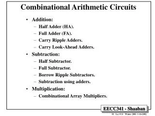
Outline • Review of Number Systems • Adders • Ripple carry • Carry Lookahead • Carry Select • Combinational Multipliers • Arithmetic and Logic Unit (ALU) • General Logic Function Units • READING: Katz 5.2.1, 5.2.2, 5.2.4, 5.3, 5.5, 4.6 ECE C03 Lecture 8
Review of Number Systems • Representation of positive numbers same in most systems • Differences in negative numbers • Three major schemes: • sign and magnitude • ones complement • twos complement • Assumptions: • we'll assume a 4 bit machine word • 16 different values can be represented • roughly half are positive, half are negative ECE C03 Lecture 8
Sign Magnitude Number System High order bit is sign: 0 = positive (or zero), 1 = negative Three low order bits is the magnitude: 0 (000) thru 7 (111) Number range for n bits = +/-2 -1 Representations for 0 Cumbersome addition/subtraction Must compare magnitudes to determine sign of result n-1 ECE C03 Lecture 8
Only one representation for 0 One more negative number than positive number Twos Complement Representation like 1's comp except shifted one position clockwise ECE C03 Lecture 8
Twos Complement Number System n N* = 2 - N 4 2 = 10000 7 = 0111 1001 = repr. of -7 sub Example: Twos complement of 7 4 2 = 10000 -7 = 1001 0111 = repr. of 7 Example: Twos complement of -7 sub Shortcut method: Twos complement = bitwise complement + 1 0111 -> 1000 + 1 -> 1001 (representation of -7) 1001 -> 0110 + 1 -> 0111 (representation of 7) ECE C03 Lecture 8
Addition and Subtraction of Numbers Sign and Magnitude 4 + 3 7 0100 0011 0111 -4 + (-3) -7 1100 1011 1111 result sign bit is the same as the operands' sign when signs differ, operation is subtract, sign of result depends on sign of number with the larger magnitude 4 - 3 1 0100 1011 0001 -4 + 3 -1 1100 0011 1001 ECE C03 Lecture 8
Twos Complement Addition and Subtraction Twos Complement Calculations 4 + 3 7 0100 0011 0111 -4 + (-3) -7 1100 1101 11001 If carry-in to sign = carry-out then ignore carry if carry-in differs from carry-out then overflow 4 - 3 1 0100 1101 10001 -4 + 3 -1 1100 0011 1111 Simpler addition scheme makes twos complement the most common choice for integer number systems within digital systems ECE C03 Lecture 8
Twos Complement Addition and Subtraction Why can the carry-out be ignored? -M + N when N > M: n n M* + N = (2 - M) + N = 2 + (N - M) n Ignoring carry-out is just like subtracting 2 n-1 -M + -N where N + M < or = 2 n n -M + (-N) = M* + N* = (2 - M) + (2 - N) = 2 - (M + N) + 2 n n After ignoring the carry, this is just the right twos compl. representation for -(M + N)! ECE C03 Lecture 8
Circuits for Binary Addition Half Adder With twos complement numbers, addition is sufficient Half-adder Schematic ECE C03 Lecture 8
Full Adder Cascaded Multi-bit Adder usually interested in adding more than two bits this motivates the need for the full adder ECE C03 Lecture 8
Full Adder S = CI xor A xor B CO = B CI + A CI + A B = CI (A + B) + A B ECE C03 Lecture 8
Full Adder Circuit Standard Approach: 6 Gates A A B B CI CO S CI A B Alternative Implementation: 5 Gates A + B A + B + CI A S S S Half Half CI (A + B) Adder Adder A B B CO CO CI CO + A B + CI (A xor B) = A B + B CI + A CI ECE C03 Lecture 8
Adder/Subtractor A B B A B B A B B A B B 3 3 3 2 2 2 1 1 1 0 0 0 S S S S 3 2 1 0 Sel 0 1 Sel 0 1 Sel 0 1 0 1 Sel A B A B A B A B Add/Subtract CO + CI CO + CI CO + CI CO + CI S S S S Overflow A - B = A + (-B) = A + B + 1 ECE C03 Lecture 8
Delay Analysis of Ripple Adder • Carry out of a single stage can be implemented in 2 gate delays • For a 16 bit adder, the 16th bit carry is generated after 16 * 2 = 32 gate delays. • The sum bit takes one additional gate delay to generate the sum of the 16th bit after 15th bit carry • 15 * 2 + 1 = 31 gate delays • Takes too long - need to investigate FASTER adders! ECE C03 Lecture 8
Carry Lookahead Adder C 0 A S @2 0 0 B C @2 0 1 A S @3 1 1 B C @4 1 2 A S @5 2 2 B C @6 2 3 A S @7 3 3 B C @8 3 4 Critical delay: the propagation of carry from low to high order stages @0 A @1 @N+1 late arriving signal B @0 CI @N CO @N+2 two gate delays to compute CO A @0 B @0 @1 0 4 stage adder 1 2 3 final sum and carry ECE C03 Lecture 8
Carry Lookahead Circuit Critical delay: the propagation of carry from low to high order stages S0, C1 Valid S1, C2 Valid S2, C3 Valid S3, C4 Valid 1111 + 0001 worst case addition T0 T2 T4 T6 T8 T0: Inputs to the adder are valid T2: Stage 0 carry out (C1) T4: Stage 1 carry out (C2) T6: Stage 2 carry out (C3) T8: Stage 3 carry out (C4) 2 delays to compute sum but last carry not ready until 6 delays later ECE C03 Lecture 8
Carry Lookahead Logic Carry Generate Gi = Ai Bi must generate carry when A = B = 1 Carry Propagate Pi = Ai xor Bi carry in will equal carry out here Sum and Carry can be reexpressed in terms of generate/propagate: Si = Ai xor Bi xor Ci = Pi xor Ci Ci+1 = Ai Bi + Ai Ci + Bi Ci = Ai Bi + Ci (Ai + Bi) = Ai Bi + Ci (Ai xor Bi) = Gi + Ci Pi ECE C03 Lecture 8
Carry Lookahead Logic Reexpress the carry logic as follows: C1 = G0 + P0 C0 C2 = G1 + P1 C1 = G1 + P1 G0 + P1 P0 C0 C3 = G2 + P2 C2 = G2 + P2 G1 + P2 P1 G0 + P2 P1 P0 C0 C4 = G3 + P3 C3 = G3 + P3 G2 + P3 P2 G1 + P3 P2 P1 G0 + P3 P2 P1 P0 C0 Each of the carry equations can be implemented in a two-level logic network Variables are the adder inputs and carry in to stage 0! ECE C03 Lecture 8
Carry Lookahead Implementation C0 C0 C0 P0 C1 P0 P0 P1 P1 G0 P2 P2 G0 P1 G0 C0 P2 P1 P0 P2 P1 G1 C3 G0 P2 C2 G1 P1 P2 G2 G1 G2 P3 Ai Pi @ 1 gate delay Bi Adder with Propagate and Generate Outputs Si @ 2 gate delays Ci Gi @ 1 gate delay Increasingly complex logic P3 P3 P3 C4 ECE C03 Lecture 8 G3
Cascaded Carry Lookahead Logic C 0 A S @2 0 0 B 0 C @3 1 A S @4 1 1 B 1 C @3 2 A S @4 2 2 B 2 C @3 3 A S @4 3 3 B 3 C @3 4 Carry lookahead logic generates individual carries sums computed much faster ECE C03 Lecture 8
Delay Analysis in Carry Lookahead • Assume a 4-stage adder with CLA • Propagate and generate signals available after 1 gate delays • Carry signals for slices 1 to 4 available after 3 gate delays • Sum signal for slices 1 to 4 after 4 gate delays ECE C03 Lecture 8
Carry Lookahead Logic A [15-12] B [15-12] A [1 1-8] B [1 1-8] A [7-4] B [7-4] A [3-0] B [3-0] C C C C C 16 4 12 8 0 4-bit Adder 4-bit Adder 4-bit Adder 4-bit Adder S [3-0] S [15-12] S [1 1-8] S [7-4] P G C P G C P G C P G 3 3 3 2 2 2 1 1 1 0 0 C C 16 C C 0 4 0 P 3-0 G 3-0 Cascaded Carry Lookahead 4 4 4 4 4 4 4 4 @0 G G G P G P P P 4 @8 4 4 @7 4 @8 @4 @2 @3 @5 @2 @3 @5 @2 @3 @4 @2 @3 Lookahead Carry Unit @5 @0 @3 @5 4 bit adders with internal carry lookahead second level carry lookahead unit, extends lookahead to 16 bits ECE C03 Lecture 8
Delay Analysis of Carry Lookahead • Consider a 16-bit adder • Implemented with four stages of 4-bit adders using carry lookahead • Carry in to the highest stage is available after 5 gate delays • Sum from highest stage available at 8 gate delays • COMPARE WITH 32 gate delays for a ripple carry adder • NOTE HOWEVER THIS ASSUMES ALL GATE DELAYS ARE SAME • Not true, delays depand on fan-ins and fan-out ECE C03 Lecture 8
Carry Select Adder • Carry Select adder trades of more hardware for faster carry propagation • Basic idea is to break up 8 bit adder into two 4-bit adder chunks • While the lowest significant 4bit adder computes carry out • In parallel have TWO high-order 4bit adders compute result with two possible cases • carry in of 0 • carry in of 1 • Depending on final result use a multiplexer to choose correct result ECE C03 Lecture 8
Carry Select Adder C Adder 8 4-Bit Adder Low [7:4] C 4 C 8 4-Bit Adder Adder [7:4] High C 4 C 4-Bit Adder ¥ 0 4 2:1 Mux [3:0] C S S S S S S S S 8 7 6 5 4 3 2 1 0 Redundant hardware to make carry calculation go faster 0 1 1 0 1 0 1 0 1 0 compute the high order sums in parallel one addition assumes carry in = 0 the other assumes carry in = 1 ECE C03 Lecture 8
Delay Analysis in Carry Select Adders • Consider an 8 bit adder using two 4 bit chunks • Assume each internal 4-bit adder uses carry lookahead • needs 4 gate delays to compute sums and 3 gate delays to compute the stage carry-out • The 2:1 multiplexers add 2 more gate delays • Hence 8-bit sum is valid after 6 gate delays • COMPARED with 7 gate delays in a carry lookahead unit and 16 gate delays of a ripple carry adder • AGAIN ASSUME that all gate delays are equal, not true in practice ECE C03 Lecture 8
Theory of Multiplication Basic Concept multiplicand multiplier 1101 (13) 1011 (11) 1101 product of 2 4-bit numbers is an 8-bit number * 1101 Partial products 0000 1101 10001111 (143) ECE C03 Lecture 8
Combinational Multiplier Partial Product Accumulation A1 B1 A1 B0 A0 B1 A0 B0 A0 B0 A3 B3 A2 B0 A2 B1 A1 B2 A0 B3 A2 B2 A2 B0 A1 B1 A0 B2 A3 B1 A2 B2 A1 B3 A3 B3 A3 B2 A2 B3 S7 S6 S4 S5 S3 S2 S1 S0 ECE C03 Lecture 8
Partial Product Accumulation Note use of parallel carry-outs to form higher order sums 12 Adders, if full adders, this is 6 gates each = 72 gates 16 gates form the partial products total = 88 gates! ECE C03 Lecture 8
Combinational Multiplier Another Representation of the Circuit Building block: full adder + and 4 x 4 array of building blocks ECE C03 Lecture 8
Arithmetic Logic Unit Design Sample ALU Logical and Arithmetic Operations Not all operations appear useful, but "fall out" of internal logic ECE C03 Lecture 8
Arithmetic Logic Unit Design M S1 S0 Ci Ai Bi 0 0 0 X 0 X X 1 X 0 1 X 0 X X 1 X 1 0 X 0 0 X 0 1 X 1 0 X 1 1 1 1 X 0 0 X 0 1 X 1 0 X 1 1 1 0 0 0 0 X 0 1 X 0 1 0 0 X 0 1 X 1 0 0 0 0 0 0 1 0 1 0 0 1 1 1 1 0 0 0 0 0 1 0 1 0 0 1 1 1 0 0 1 0 X 1 1 X 0 1 1 0 X 1 1 X 1 0 1 0 0 1 0 1 1 1 0 1 1 1 1 1 0 1 0 1 1 1 1 Sample ALU Fi Ci+1 Traditional Design Approach 0 X 1 X 1 X 0 X Truth Table & Espresso 0 X 1 X 1 X .i 6 .o 2 .ilb m s1 s0 ci ai bi .ob fi co .p 23 111101 10 110111 10 1-0100 10 1-1110 10 10010- 10 10111- 10 -10001 10 010-01 10 -11011 10 011-11 10 --1000 10 0-1-00 10 --0010 10 0-0-10 10 -0100- 10 001-0- 10 -0001- 10 000-1- 10 -1-1-1 01 --1-01 01 --0-11 01 --110- 01 --011- 01 .e 0 X 1 X 23 product terms! 0 X 0 X 1 X 0 X 1 X Equivalent to 25 gates 1 X 0 X 0 0 1 0 1 0 0 1 1 0 0 1 0 0 1 0 1 0 0 1 0 1 1 0 1 0 0 1 0 1 1 1 1 0 0 1 1 1 1 ECE C03 Lecture 8 0 1 0 1 0 1
Arithmetic Logic Unit Design Sample ALU Multilevel Implementation .model alu.espresso .inputs m s1 s0 ci ai bi .outputs fi co .names m ci co [30] [33] [35] fi 110--- 1 -1-11- 1 --01-1 1 --00-0 1 .names m ci [30] [33] co -1-1 1 --11 1 111- 1 .names s0 ai [30] 01 1 10 1 .names m s1 bi [33] 111 1 .names s1 bi [35] 0- 1 -0 1 .end \S1 M [35] Ci Ci \Bi [33] \Co Ci [30] M [30] Co [33] S1 [33] [33] Fi Bi \Co M [30] Ci [35] [30] S0 \Co [30] Ai \[30] \[35] 12 Gates ECE C03 Lecture 8
Arithmetic Logic Unit Design Sample ALU Clever Multi-level Logic Implementation S1 = 0 blocks Bi Happens when operations involve Ai only Same is true for Ci when M = 0 Addition happens when M = 1 Bi, Ci to Xor gates X2, X3 S0 = 0, X1 passes A S0 = 1, X1 passes A S1 Bi S0 Ai M Ci X1 A1 A2 X2 A3 A4 Arithmetic Mode: Or gate inputs are Ai Ci and Bi (Ai xor Ci) X3 O1 Logic Mode: Ci+1 Fi Cascaded XORs form output from Ai and Bi ECE C03 Lecture 8 8 Gates (but 3 are XOR)
Arithmetic Logic Unit Design 74181 TTL ALU ECE C03 Lecture 8
Arithmetic Logic Unit Design 74181 TTL ALU Note that the sense of the carry in and out are OPPOSITE from the input bits 19 182 A3 21 13 6 A2 F3 181 P3 23 11 A1 F2 15 P2 2 10 7 A0 F1 P 2 18 9 P1 B3 F0 10 G 20 4 B2 P0 14 A=B 22 B1 5 16 G3 Cn+4 9 1 Cn+z B0 14 G2 17 11 G Cn+y 7 Cn 1 15 G1 P 12 8 Cn+x M 3 G0 S3 S2 S1 S0 13 Cn 3 4 5 6 Fortunately, carry lookahead generator maintains the correct sense of the signals ECE C03 Lecture 8
Arithmetic Logic Unit Design 19 A3 21 13 A2 181 F3 23 11 A1 F2 2 10 A0 F1 18 9 B3 F0 20 B2 14 A=B 22 B1 16 Cn+4 1 B0 17 G 7 Cn P 15 8 M S3 S2 S1 S0 3 4 5 6 19 A3 21 13 A2 181 F3 23 11 A1 F2 2 10 A0 F1 18 9 B3 F0 20 B2 14 A=B 22 B1 16 Cn+4 1 B0 17 G 7 Cn P 15 182 8 M 6 P3 15 P2 S3 S2 S1 S0 7 2 P P1 3 4 5 6 10 4 G P0 5 G3 19 A3 9 14 Cn+z G2 21 13 A2 181 F3 11 1 Cn+y G1 23 11 12 A1 F2 3 Cn+x G0 2 10 A0 F1 18 9 B3 13 F0 Cn 20 B2 14 A=B 22 B1 16 Cn+4 1 B0 17 G 7 Cn 15 P 8 M S3 S2 S1 S0 3 4 5 6 A3 A2 181 A1 A0 B3 B2 B1 B0 Cn M S3 S2 S1 16-bit ALU with Carry Lookahead C16 19 21 13 F3 23 11 F2 2 10 F1 18 9 F0 20 14 A=B 22 16 Cn+4 1 C0 17 G 7 15 P 8 S0 3 4 5 6 ECE C03 Lecture 8
General Logical Function Unit Statement of the Problem: 3 control inputs: C0, C1, C2 2 data inputs: A, B 1 output: F Similar to the main computation unit in a Microprocessor ECE C03 Lecture 8
Logical Function Unit + 5 V C D D D D D D D D S 2 0 1 2 3 4 5 6 7 0 C S E 1 1 N C Q S 0 O 2 Formulate as a truth table Choose implementation technology 4 TTL packages: 4 x 2-input NAND 4 x 2-input NOR 2 x 2-input XOR 8:1 MUX A B A B A B 8:1 Mux F ECE C03 Lecture 8
Logical Function Unit C C 1 2 C =0 0 C C 1 2 C =1 0 Follow implementation procedure A B 00 01 11 10 00 1 1 F = C2' A' B' + C0' A B' + C0' A' B + C1' A B 01 1 1 1 1 5 gates, 5 inverters Also four packages: 4 x 3-input NAND 1 x 4-input NAND Alternative: PAL/PLA single package 11 1 1 10 1 1 1 1 A B 00 01 11 10 1 1 00 01 11 1 1 10 ECE C03 Lecture 8
Summary • Review of Arithmetic Number Representation • Adders - Ripple carry, Carry Lookahead, Carry Select Adders • Combinational multipliers • Arithmetic and Logic Unit (ALU) • General function circuits • NEXT LECTURE: Memory Elements and Clocking • READING: Katz 6.1, 6.2, 6.3, Dewey 8.1, 8.2 ECE C03 Lecture 8