Download

1 / 76
770 likes | 902 Vues
Lecture 6 Combinational Arithmetic Circuits. Pradondet Nilagupta Department of Computer Engineering Kasetsart University. Acknowledgement.

E N D
Lecture 6 Combinational Arithmetic Circuits Pradondet Nilagupta Department of Computer Engineering Kasetsart University
Acknowledgement • This lecture note is modified from EECC 341 – Introduction to Digital System for Computer Engineering from Dr. Muhammad Shaaban and ECE 303 Advanced Digital Design from Prof. Hai Zhou • http://www.rit.edu/~meseec/eecc341-winter2001/ • http://www.ece.nwu.edu/~haizhou/ece303.html 204222 Digital System Design
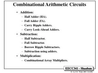
Combinational Arithmetic Circuits • Addition: • Half Adder (HA). • Full Adder (FA). • Carry Ripple Adders. • Carry Look-Ahead Adders. • Subtraction: • Half Subtractor. • Full Subtractor. • Borrow Ripple Subtractors. • Subtraction using adders. • Multiplication: • Combinational Array Multipliers. 204222 Digital System Design
X 0 0 1 1 Y 0 1 0 1 S 0 1 1 0 C-out 0 0 0 1 Half Adder Truth Table Outputs Inputs X Half Adder S C-OUT Y Half Adder • Adding two single-bit binary values, X, Y produces a sum S bit and a carry out C-out bit. • This operation is called half addition and the circuit to realize it is called a half adder. • S(X,Y) = S (1,2) • S = X’Y + XY’ • S = X Å Y • C-out(x, y, C-in) = S (3) • C-out = XY X Y Sum S C-out 204222 Digital System Design
X 0 0 0 0 1 1 1 1 Y 0 0 1 1 0 0 1 1 C-in 0 1 0 1 0 1 0 1 S 0 1 1 0 1 0 0 1 C-out 0 0 0 1 0 1 1 1 Full Adder • Adding two single-bit binary values, X, Y with a carry input bit C-in produces a sum bit S and a carry out C-out bit. Full Adder Truth Table Outputs Inputs • S(X,Y, C-in) = S (1,2,4,7) • C-out(x, y, C-in) = S (3,5,6,7) 204222 Digital System Design
Sum S X X XY XY 00 01 11 10 00 01 11 10 C-in C-in 1 1 6 6 0 0 2 2 4 4 0 1 0 1 1 1 3 3 5 5 7 7 1 1 C-in C-in Carry C-out Y Y 1 1 1 1 Full Adder S = X’Y’(C-in) + XY’(C-in)’ + XY’(C-in)’ + XY(C-in) S = X Å Y Å(C-in) C-out = XY + X(C-in) + Y(C-in) 204222 Digital System Design
X’ X’Y’C-in Y’ C-in X Y Y X X’ Sum S X’YC-in’ Y X X’ Y’ Y C-in’ Full Adder C-out C-in X C-in Y C-in C-in’ C-in’ XY’C-in’ X S Y XYC-in C-in’ X XY Y X XC-in C-out C-in Y YC-in C-in Full Adder Circuit Using AND-OR 204222 Digital System Design
X Y Sum S X Full Adder C-out C-in Y C-in S X XY Y X XC-in C-out C-in Y YC-in C-in Full Adder Circuit Using XOR 204222 Digital System Design
n-bit Carry Ripple Adders • An n-bit adder used to add two n-bit binary numbers can built by connecting in series n full adders. • Each full adder represents a bit position j (from 0 to n-1). • Each carry out C-out from a full adder at position j is connected to the carry in C-in of the full adder at the higher position j+1. • The output of a full adder at position j is given by: Sj = XjÅ YjÅCj Cj+1 = Xj . Yj + Xj . Cj + Y . Cj 204222 Digital System Design
n-bit Carry Ripple Adders • In the expression of the sum Cj must be generated by the full adder at the lower position j-1. • The propagation delay in each full adder to produce the carry is equal to two gate delays = 2 D • Since the generation of the sum requires the propagation of the carry from the lowest position to the highest position , the total propagation delay of the adder is approximately: Total Propagation delay = 2 nD 204222 Digital System Design
Inputs to be added X3X2X1X0 Y3Y2Y1Y0 4-bit Adder C4 C0 =0 C-in C-out X0 Y0 X1 X2 X3 Y3 Y2 Y1 S3 S2 S1 S0 Full Adder Full Adder Full Adder Full Adder C3 C2 C1 Data inputs to be added C4 C0 =0 C-in C-in C-in C-in C-out C-out C-out C-out Sum Output S0 S2 S3 S1 Sum output 4-bit Carry Ripple Adder Adds two 4-bit numbers: X = X3 X2 X1 X0 Y = Y3 Y2 Y1 Y0 producing the sum S = S3 S2 S1 S0 , C-out = C4 from the most significant position j=3 Total Propagation delay = 2 nD = 8D or 8 gate delays 204222 Digital System Design
Data inputs to be added X (X0 to X15) , Y (Y0-Y15) 4-bit Adder 4-bit Adder 4-bit Adder 4-bit Adder C12 C8 C4 C16 C0 =0 C-in C-in C-in C-in C-out C-out C-out C-out Sum output S (S0 to S15) Y3Y2Y1Y0 Y3Y2Y1Y0 Y3Y2Y1Y0 Y3Y2Y1Y0 X3X2X1X0 X3X2X1X0 X3X2X1X0 X3X2X1X0 S3 S2 S1 S0 S3 S2 S1 S0 S3 S2 S1 S0 S3 S2 S1 S0 Larger Adders • Example: 16-bit adder using 4, 4-bit adders • Adds two 16-bit inputs X (bits X0 to X15), Y (bits Y0 to Y15) producing a 16-bit Sum S (bits S0 to S15) and a carry out C16 from most significant position. Propagation delay for 16-bit adder = 4 x propagation delay of 4-bit adder = 4 x 2 nD = 4 x 8D = 32D or 32 gate delays 204222 Digital System Design
Carry Look-Ahead Adders • The disadvantage of the ripple carry adder is that the propagation delay of adder (2 nD ) increases as the size of the adder, n is increased due to the carry ripple through all the full adders. • Carry look-ahead adders use a different method to create the needed carry bits for each full adder with a lower constant delay equal to three gate delays. • The carry out C-out from the full adder at position i or Cj+1 is given by: C-out = C i+1 = Xi . Yi + (Xi + Yi) . Ci 204222 Digital System Design
Carry Look-Ahead Adders • By defining: • Gi = Xi . Yi as the carry generate function for position i (one gate delay) (If Gi =1 C i+1 will be generated regardless of the value Ci) • Pi = Xi + Yi as the carry propagate function for position i (one gate delay) (If Pi = 1 Ci will be propagated to C i+1) 204222 Digital System Design
Carry Look-Ahead Adders • By using the carry generate function Gi and carry propagate function Pi , then C i+1 can be written as: C-out = C i+1 = Gi + Pi . Ci • To eliminate carry ripple the term Ci is recursively expanded and by multiplying out, we obtain a 2-level AND-OR expression for each C i+1 204222 Digital System Design
Carry Look-Ahead Adders • For a 4-bit carry look-ahead adder the expanded expressions for all carry bits are given by: C1 = G0 + P0.C0 C2 = G1 + P1.C1 = G1 + P1.G0 + P1.P0.C0 C3 = G2 + P2.G1 + P2.P1.G0 + P2.P1.P0.C0 C4 = G3 + P3.G2 + P3.P2.G1 + P3 .P2.P1.G0 + P3.P2.P1.P0.C0 where Gi = Xi . Yi Pi = Xi + Yi 204222 Digital System Design
Carry Look-Ahead Adders • The additional circuits needed to realize the expressions are usually referred to as the carry look-ahead logic. • Using carry-ahead logic all carry bits are available after three gate delays regardless of the size of the adder. 204222 Digital System Design
Carry Look-Ahead Circuit Ci = Gi-1 + Pi-1. Gi-2 + …. + Pi-1.P i-2. …P1 . G0 + P i-1.P i-2. …P0 . C0 204222 Digital System Design
C0 C0 C0 P0 C1 P0 P0 P1 P1 G0 P2 P2 G0 P1 G0 C0 P2 P1 P0 P2 P1 G1 C3 G0 P2 C2 G1 P1 P2 G2 G1 G2 P3 Carry Lookahead Implementation Ai Pi @ 1 gate delay Bi Adder with Propagate and Generate Outputs Si @ 2 gate delays Ci Gi @ 1 gate delay Increasingly complex logic P3 P3 P3 C4 G3 204222 Digital System Design
C 0 A S @2 0 0 B 0 C @3 1 A S @4 1 1 B 1 C @3 2 A S @4 2 2 B 2 C @3 3 A S @4 3 3 B 3 C @3 4 Cascaded Carry Lookahead Logic Carry lookahead logic generates individual carries sums computed much faster 204222 Digital System Design
Delay Analysis in Carry Lookahead • Assume a 4-stage adder with CLA • Propagate and generate signals available after 1 gate delays • Carry signals for slices 1 to 4 available after 3 gate delays • Sum signal for slices 1 to 4 after 4 gate delays 204222 Digital System Design
A [15-12] B [15-12] A [1 1-8] B [1 1-8] A [7-4] B [7-4] A [3-0] B [3-0] C C C C C 16 4 12 8 0 4-bit Adder 4-bit Adder 4-bit Adder 4-bit Adder S [3-0] S [15-12] S [1 1-8] S [7-4] P G C P G C P G C P G 3 3 3 2 2 2 1 1 1 0 0 C C 16 C C 0 4 0 P 3-0 G 3-0 Carry Lookahead Logic Cascaded Carry Lookahead 4 4 4 4 4 4 4 4 @0 G G G P G P P P 4 @8 4 4 @7 4 @8 @4 @2 @3 @5 @2 @3 @5 @2 @3 @4 @2 @3 Lookahead Carry Unit @5 @0 @3 @5 4 bit adders with internal carry lookahead second level carry lookahead unit, extends lookahead to 16 bits 204222 Digital System Design
Delay Analysis of Carry Lookahead • Consider a 16-bit adder • Implemented with four stages of 4-bit adders using carry lookahead • Carry in to the highest stage is available after 5 gate delays • Sum from highest stage available at 8 gate delays • COMPARE WITH 32 gate delays for a ripple carry adder • NOTE HOWEVER THIS ASSUMES ALL GATE DELAYS ARE SAME • Not true, delays depand on fan-ins and fan-out 204222 Digital System Design
Binary Arithmetic OperationsSubtraction • Two binary numbers are subtracted by subtracting each pair of bits together with borrowing, where needed. • Subtraction Example: Borrow 0 0 1 1 1 1 1 0 0 X 229 1 1 1 0 0 1 0 1 Y - 46 - 0 0 1 0 1 1 1 0 183 1 0 1 1 0 1 1 1 204222 Digital System Design
X 0 0 1 1 Y 0 1 0 1 D 0 1 1 0 B-out 0 1 0 0 Half Subtractor Truth Table Outputs Inputs X Half Subtractor D B-OUT Y Half Subtractor • Subtracting a single-bit binary value Y from anther X (I.e. X -Y ) produces a difference bit D and a borrow out bit B-out. • This operation is called half subtraction and the circuit to realize it is called a half subtractor. • D(X,Y) = S (1,2) • D = X’Y + XY’ • D = X Å Y • B-out(x, y, C-in) = S (1) • B-out = X’Y Difference D X Y B-out 204222 Digital System Design
X 0 0 0 0 1 1 1 1 Y 0 0 1 1 0 0 1 1 B-in 0 1 0 1 0 1 0 1 D 0 1 1 0 1 0 0 1 B-out 0 1 1 1 0 0 0 1 Full Subtractor • Subtracting two single-bit binary values, Y, B-in from a single-bit value X produces a difference bit D and a borrow out B-out bit. This is called full subtraction. Full Subtractor Truth Table Outputs Inputs • S(X,Y, C-in) = S (1,2,4,7) • C-out(x, y, C-in) = S (1,2,3,7) 204222 Digital System Design
Difference D X X XY XY 00 01 11 10 00 01 11 10 B-in B-in 1 1 6 6 0 0 2 2 4 4 0 1 0 1 1 1 3 3 5 5 7 7 1 1 B-in B-in Y Y Full Subtractor S = X’Y’(B-in) + XY’(B-in)’ + XY’(B-in)’ + XY(B-in) S = X Å Y Å(C-in) Borrow B-out 1 1 1 1 B-out = X’Y + X’(B-in) + Y(B-in) 204222 Digital System Design
X’ X’Y’B-in Y’ B-in X Y X’ Difference D X’YB-in’ X Y X’ Y’ Y B-in’ X B-in Y B-in B-in’ B-in’ XY’B-in’ X Y XYB-in B-in’ X Y X’ X’Y Y Full Subtractor B-out B-in X’ X’B-in B-out B-in Y D YB-in B-in Full Subtractor Circuit Using AND-OR 204222 Digital System Design
X Y B-in X Y X’ X’Y Y Full Subtractor B-out B-in X’ X’B-in B-out B-in Y D YB-in B-in Full Subtractor Circuit Using XOR Difference D 204222 Digital System Design
n-bit Subtractors • An n-bit subtracor used to subtract an n-bit number Y from another n-bit number X (i.e X-Y) can be built in one of two ways: • By using n full subtractors and connecting them in series, creating a borrow ripple subtractor: • Each borrow out B-out from a full subtractor at position j is connected to the borrow in B-in of the full subtracor at the higher position j+1. 204222 Digital System Design
n-bit Subtractors • By using an n-bit adder and n inverters: • Find two’s complement of Y by: • Inverting all the bits of Y using the n inverters. • Adding 1 by setting the carry in of the least significant position to 1 • The original subtraction (X - Y) now becomes an addition of X to two’s complement of Y using the n-bit adder. 204222 Digital System Design
Inputs X3X2X1X0 Y3Y2Y1Y0 4-bit Subtractor B4 B0 =0 B-in B-out D3 D2 D1 D0 Difference Output D Data inputs to be subtracted X3 Y3 X2 Y2 X1 Y1 X0 Y0 B3 B2 B1 Full Subtractor Full Subtractor Full Subtractor Full Subtractor B4 B0 =0 B-in B-in B-in B-in B-out B-out B-out B-out D3 D2 D1 D0 Difference output D 4-bit Borrow Ripple Subtractor Subtracts two 4-bit numbers: Y = Y3 Y2 Y1 Y0 from X = X3 X2 X1 X0 Y = Y3 Y2 Y1 Y0 producing the difference D = D3 D2 D1 D0 , B-out = B4 from the most significant position j=3 204222 Digital System Design
4-bit Subtractor Using 4-bit Adder Inputs to be subtracted Y3 Y2 Y1 Y0 X3 X2 X1 X0 4-bit Adder C4 C0 = 1 C-out C-in S3 S2 S1 S0 D3 D2 D1 D0 Difference Output 204222 Digital System Design
A B B A B B A B B A B B 3 3 3 2 2 2 1 1 1 0 0 0 S S S S 3 2 1 0 Adder/Subtractor Sel 0 1 Sel 0 1 Sel 0 1 0 1 Sel A B A B A B A B Add/Subtract CO + CI CO + CI CO + CI CO + CI S S S S Overflow A - B = A + (-B) = A + B + 1 204222 Digital System Design
Binary Multiplication • Multiplication is achieved by adding a list of shifted multiplicands according to the digits of the multiplier. • Ex. (unsigned) 11 1 0 1 1 multiplicand (4 bits) X 13 X 1 1 0 1 multiplier (4 bits) -------- ------------------- 33 1 0 1 1 11 0 0 0 0 ______ 1 0 1 1 143 1 0 1 1 --------------------- 1 0 0 0 1 1 1 1 Product (8 bits) 204222 Digital System Design
Binary Multiplication • An n-bit X n-bit multiplier can be realized in combinational circuitry by using an array of n-1 n-bit adders where is adder is shifted by one position. • For each adder one input is the multiplied by 0 or 1 (using AND gates) depending on the multiplier bit, the other input is n partial product bits. X3 X2 X1 X0 x Y3 Y2 Y1 Y0 __________________________ X3.Y0 X2.Y0 X1.Y0 X0.Y0 X3.Y1 X2.Y1 X1.Y1 X0.Y1 X3.Y2 X2.Y2 X1.Y2 X0.Y2 X3.Y3 X2.Y3 X1.Y3 X0.Y3 _______________________________________________________________________________________________________________________________________________ P7 P6 P5 P4 P3 P2 P1 P0 204222 Digital System Design
4x4 Array Multiplier 204222 Digital System Design
Combinational Multiplier Partial Product Accumulation A1 B1 A1 B0 A0 B1 A0 B0 A0 B0 A3 B3 A2 B0 A2 B1 A1 B2 A0 B3 A2 B2 A2 B0 A1 B1 A0 B2 A3 B1 A2 B2 A1 B3 A3 B3 A3 B2 A2 B3 S7 S6 S4 S5 S3 S2 S1 S0 204222 Digital System Design
Partial Product Accumulation Note use of parallel carry-outs to form higher order sums 12 Adders, if full adders, this is 6 gates each = 72 gates 16 gates form the partial products total = 88 gates! 204222 Digital System Design
Combinational Multiplier Another Representation of the Circuit Building block: full adder + and 4 x 4 array of building blocks 204222 Digital System Design
Full-adder array 204222 Digital System Design
Faster carry chain 204222 Digital System Design
Arithmetic Logic Unit Design Sample ALU Logical and Arithmetic Operations Not all operations appear useful, but "fall out" of internal logic 204222 Digital System Design
M S1 S0 Ci Ai Bi 0 0 0 X 0 X X 1 X 0 1 X 0 X X 1 X 1 0 X 0 0 X 0 1 X 1 0 X 1 1 1 1 X 0 0 X 0 1 X 1 0 X 1 1 1 0 0 0 0 X 0 1 X 0 1 0 0 X 0 1 X 1 0 0 0 0 0 0 1 0 1 0 0 1 1 1 1 0 0 0 0 0 1 0 1 0 0 1 1 1 0 0 1 0 X 1 1 X 0 1 1 0 X 1 1 X 1 0 1 0 0 1 0 1 1 1 0 1 1 1 1 1 0 1 0 1 1 1 1 Arithmetic Logic Unit Design Sample ALU Fi Ci+1 Traditional Design Approach 0 X 1 X 1 X 0 X Truth Table & Espresso 0 X 1 X 1 X .i 6 .o 2 .ilb m s1 s0 ci ai bi .ob fi co .p 23 111101 10 110111 10 1-0100 10 1-1110 10 10010- 10 10111- 10 -10001 10 010-01 10 -11011 10 011-11 10 --1000 10 0-1-00 10 --0010 10 0-0-10 10 -0100- 10 001-0- 10 -0001- 10 000-1- 10 -1-1-1 01 --1-01 01 --0-11 01 --110- 01 --011- 01 .e 0 X 1 X 23 product terms! 0 X 0 X 1 X 0 X 1 X Equivalent to 25 gates 1 X 0 X 0 0 1 0 1 0 0 1 1 0 0 1 0 0 1 0 1 0 0 1 0 1 1 0 1 0 0 1 0 1 1 1 1 0 0 1 1 1 1 0 1 0 204222 Digital System Design 1 0 1
Arithmetic Logic Unit Design Sample ALU Multilevel Implementation .model alu.espresso .inputs m s1 s0 ci ai bi .outputs fi co .names m ci co [30] [33] [35] fi 110--- 1 -1-11- 1 --01-1 1 --00-0 1 .names m ci [30] [33] co -1-1 1 --11 1 111- 1 .names s0 ai [30] 01 1 10 1 .names m s1 bi [33] 111 1 .names s1 bi [35] 0- 1 -0 1 .end \S1 M [35] Ci Ci \Bi [33] \Co Ci [30] M [30] Co [33] S1 [33] [33] Fi Bi \Co M [30] Ci [35] [30] S0 \Co [30] Ai \[30] \[35] 12 Gates 204222 Digital System Design
Programmable Arrays of Logic Gates • Until now, we learned about designing Boolean functions using discrete logic gates • We will now describe a technique to arrange AND and OR gates (or NAND and NOR gates) into a general array structure • Specific functions can be programmed • Can use programmable logic arrays (PLA) or programmable array logic (PAL) 204222 Digital System Design
PALs and PLAs Pre-fabricated building block of many AND/OR gates (or NOR, NAND) "Personalized" by making or breaking connections among the gates Programmable Array Block Diagram for Sum of Products Form 204222 Digital System Design
Programmable Logic Arrays (PLAs) • Any combinational logic function can be realized as a sum of products. • Idea: Build a large AND-OR array with lots of inputs and product terms, and programmable connections. • n inputs • AND gates have 2n inputs -- true and complement of each variable. • m outputs, driven by large OR gates • Each AND gate is programmably connected to each output’s OR gate. • p AND gates (p<<2n) 204222 Digital System Design
Why PALs/PLAs Work Equations F0 = A + B' C' F1 = A C' + A B F2 = B' C' + A B F3 = B' C + A Example: Key to Success: Shared Product Terms Personality Matrix Input Side: 1 = asserted in term 0 = negated in term - = does not participate Output Side: 1 = term connected to output 0 = no connection to output 204222 Digital System Design
Example of PALs and PLAs All possible connections are available before programming 204222 Digital System Design