Download
1 / 29
290 likes | 434 Vues
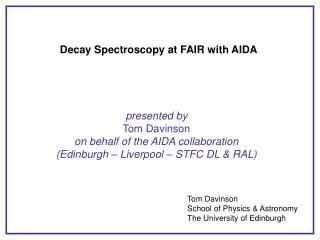
Decay Spectroscopy at FAIR Using the Advanced Implantation Detector Array (AIDA). presented by Tom Davinson on behalf of the AIDA collaboration (Edinburgh – Liverpool – CCLRC DL & RAL). Tom Davinson School of Physics The University of Edinburgh. Presentation Outline. Where? Why?

E N D
Decay Spectroscopy at FAIR Using the Advanced Implantation Detector Array (AIDA) presented by Tom Davinson on behalf of the AIDA collaboration (Edinburgh – Liverpool – CCLRC DL & RAL) Tom Davinson School of Physics The University of Edinburgh
Presentation Outline • Where? • Why? • How? • When? • Who? • What next?
FAIR: Facility for Antiproton and Ion Research GSI today Future facility 100 m SIS 100/300 SIS 18 UNILAC ESR • Cost • Approx €1000M • €650M central German government • €100M German regional funding • €250M from international partners • Timescale • Feb 2006- German funds in budget 2007-14 • 2007 start construction • 2012 phased start experiments • 2014 completion HESR Super FRS RESR NUSTAR NESR
NUSTAR: Nuclear Structure Astrophysics & Reactions Exotic (radioactive) beams formed by fragmentation, selected by separator. HiSpec :gamma spec DeSpec :decay spec LASPEC: laser spec MATS: Penning traps R3B: reactions Stored beam (rings): EXL : hadron scattering ELISe : electron scattering AIC : antiproton scattering
FAIR: Production Rates Predicted Lifetimes > 100ns from FAIR CDR, section 2
r-process • Nucleosynthesis along neutron-rich side of valley of stability • via s-process and r-process • s-process – Red Giants, long timescales, moderate n-flux • nucleosynthesis close to valley • r-process – Supernova type II?, timescales ~seconds?, high n-flux? • nucleosynthesis far from valley • equilibrium (n,g) and (g,n) reactions? • n-capture until binding energy becomes small • wait for b decay to nuclei with higher binding energy • effect of neutron magic numbers – 82, 126? • Require: • nuclear masses (r-process pathway) • b decay half lives (abundance along pathway) • b-delayed neutron emission probabilities (abundance modification)
NUSTAR: DESPEC/HISPEC Note – this layout is so out of date …
DESPEC: Implantation DSSD Concept • SuperFRS, Low Energy Branch (LEB) • Exotic nuclei – energies ~ 50 – 200MeV/u • Implanted into multi-plane, highly segmented DSSD array • Implant – decay correlations • Multi-GeV DSSD implantation events • Observe subsequent p, 2p, a, b, g, bp, bn … decays • Measure half lives, branching ratios, decay energies … • Tag interesting events for gamma and neutron detector arrays
Implantation DSSD Configurations • Two configurations proposed: • 8cm x 24cm • “cocktail” mode • many isotopes measured simultaneously • b) 8cm x 8cm • high efficiency mode • concentrate on particular isotope(s)
Implantation – Decay Correlation • DSSD strips identify where (x,y) and when (t0) ions implanted • Correlate with upstream detectors to identify implanted ion type • Correlate with subsequent decay(s) at same position (x,y) at times t1(,t2, …) • Observation of a series of correlations enables determination of energy • distribution and half-life of radioactive decay • Require average time between implants at position (x,y) >> decay half-life • depends on DSSD segmentation and implantation rate/profile • Implantation profile • sx ~ sy ~ 2cm, sz ~ 1mm • Implantation rate (8cm x 24cm) ~ 10kHz, ~ kHz per isotope (say) • Longest half life to be observed ~ seconds • Implies quasi-pixel dimensions ~ 0.5mm x 0.5mm
Silicon Detector Technology • Current Technology • Single, double-sided, resistive strip • Thin Junctions • p+ 0.1mm cf. ~ 0.4mm • Integrated Components • Coupling Capacitors • Bias Resistors • 3” & 4” Wafers • Thicknesses ~ 20 – 1500mm • Max. Area ~ 70cm2 • 6” Wafers • Thicknesses ~ 200 – 700mm • Max. Area ~ 160cm2 • MSL type YY1 (LEDA) • d.c. single sided • 8 sectors, 16 strips/sector • Strip Pitch 5mm • Area 370cm2 • NIM A454 (2000) 350
Silicon Detector Technology contd. GLAST Large Area Telescope (LAT) • Layers of silicon detectors interleaved with heavy-metal converters for > 20MeV g-rays • Area~80 m2 • ~106 channels • integrated a.c. coupling and bias resistors • series strip bonding • >10000 wafers from Hamamatsu Very high quality: • Leakage current < 2.5 nA/cm2 • Bad channels < 1/10,000 • Full depletion < 100 V 8.95 cm square Hamamatsu-Photonics SSD before cutting from the 6-inch wafer. The thickness is 400 microns, and the strip pitch is 228 microns.
AIDA: DSSD Array Design Implantation depth? Stopping power? Ge b detector? Calibration? Radiation damage? Cooling? courtesy B.Rubio • 8cm x 8cm DSSDs • common wafer design for 8cm x 24cm and 8cm x 8cm configurations • 8cm x 24cm • 3 adjacent wafers – horizontal strips series bonded • 128 p+n junction strips, 128 n+n ohmic strips per wafer • strip pitch 625mm • wafer thickness 1mm • DE, Veto and up to 6 intermediate planes • 4096 channels (8cm x 24cm) • overall package sizes (silicon, PCB, connectors, enclosure … ) • ~ 10cm x 26cm x 4cm or ~ 10cm x 10cm x 4cm
ASIC Design Requirements Selectable gain 20 100020000 MeV FSR Low noise 12 60050000 keV FWHM energy measurement of implantation and decay events Selectable threshold < 0.25 – 10% FSR observe and measure low energy b, b detection efficiency Integral non-linearity < 0.1% and differential non-linearity < 2% for > 95% FSR spectrum analysis, calibration, threshold determination Autonomous overload detection & recovery ~ ms observe and measure fast implantation – decay correlations Nominal signal processing time < 10ms observe and measure fast decay – decay correlations Receive (transmit) timestamp data correlate events with data from other detector systems Timing trigger for coincidences with other detector systems DAQ rate management, neutron ToF
Schematic of Prototype ASIC Functionality • Note – prototype ASIC will also evaluate use of digital signal processing • Potential advantages • decay – decay correlations to ~ 200ns • pulse shape analysis • ballistic deficit correction
Representative ASIC Noise Analysis Note – amongst other assumptions, we assume detector cooling • Minimise ballistic deficit • shaping time >10x tr • operate with t ~ ms • noise dominated by leakage current for ID > 10 nA
Design Study Conclusions • 4’’ or 6” Si wafer technology? • - integrated polysilicon bias resistors (15MW) • - separate coupling capacitors (require 22nF/200V+) • Radiation damage mitigation measures essential • - detector cooling required • Noise specification (12keV FWHM) … “not unreasonable” • Discriminator • - low threshold (<50keV) – slow, compromised for ID > 100nA • - separate timing discriminator – higher threshold • x1000 overload recovery ~ ms achievable • - depends on input pulse shape • - optimisation requires more information
Front End Electronics (FEE) Concept 16 FADCs (12 bit) 1 Sliding Scale ADC (14bit) per ASIC 128 detector signals in; 1 data fibre out 16 ch ASIC 16 FADCs ASIC Virtex 4FX FPGA Power Supplies, Temperature+ voltage monitors and other components 1 SS ADC ASIC 16 FADCs 1 SS ADC ADC Readout ASIC 16 FADCs 1 SS ADC Timestamp control 16 FADCs ASIC FADC PSA 1 SS ADC ASIC 16 FADCs ASIC Control 1 SS ADC Slow Control ASIC 16 FADCs 1 SS ADC Data Output Fibre Driver (Laser) Ethernet physical interface 16 FADCs ASIC PPC (Unix) 1 SS ADC ASIC 16 FADCs 1 SS ADC courtesy Ian Lazarus, CCLRC DL
FEE Detail for One ASIC courtesy Ian Lazarus, CCLRC DL Part of FPGA Octal FADC (serial out) 12bit 50MHz (2 per ASIC) Octal FADC (serial out) 12bit 50MHz (2 per ASIC) Pk Det & Mux Preamp + shaper low/high gain. (16 channels) Sliding Scale Spectroscopy ADC 14bits 1 to 5us conv. Control Logic
AIDA: System Concept BUTIS Timestamps PC Farm Data Output Switch Slow Control courtesy I.Lazarus, CCLRC DL
AIDA Design Concept Detail of DSSSD detector layers and detector enclosure Beam courtesy Dave Seddon & Rob Page, University of Liverpool
AIDA Design Concept AIDA instrumentation (beige) Heavy-metal shielding (grey) courtesy Dave Seddon & Rob Page, University of Liverpool
AIDA: Current Status • Edinburgh – Liverpool – CCLRC DL – CCLRC RAL collaboration • - 4 year grant period • - DSSD design, prototype and production • - ASIC design, prototype and production • - Integrated Front End FEE PCB development and production • - Systems integration • - Software development • Deliverable: fully operational DSSD array to DESPEC • Proposal approved EPSRC Physics Prioritisation panel meeting April 2006 • Project commenced August 2006 • Detailed specification development underway • M0 – specification finalised and critical review • Technical Specification release to project engineers January 2007 We are here!
AIDA: Resources & Tasks • Cost • Total announced value proposal £1.96M • Support Manpower • CCLRC DL c. 4.2 SY FEE PCB Design • DAQ h/w & s/w • CCLRC RAL c. 3.5 SY ASIC Design & simulation • ASIC Production • Edinburgh/Liverpool c. 4.5 SY DSSD Design & production • FEE PCB production • Mechanical housing/support • Platform grant support CCLRC DL/Edinburgh/Liverpool
AIDA: Project Partners • The University of Edinburgh (lead RO) • Phil Woods et al. • The University of Liverpool • Rob Page et al. • CCLRC DL & RAL • John Simpson et al. • Project Manager: Tom Davinson • Further information:http://www.ph.ed.ac.uk/~td/AIDA • Technical Specification: • http://www.ph.ed.ac.uk/~td/AIDA/Design/AIDA_Draft_Technical_Specification_v1.pdf • Comments on Technical Specification invited!
Acknowledgements This presentation includes material from other people Thanks to: Ian Lazarus (CCLRC DL) Steve Thomas (CCLRC RAL) Dave Seddon & Rob Page (University of Liverpool) Berta Rubio (IFIC, CSIC University of Valencia) Haik Simon (GSI)