Download
1 / 22
220 likes | 407 Vues
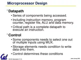
Design Of A 16 bit RISC Microprocessor Using Multi-Cycle Data path. By Praveen Venkataramani. Instruction set architecture. Maximum allowable instruction N =16 Number of op-code bits = log 2 N = log 2 16 = 4 bits Number of bits in the instruction word = 16 bits

E N D
Design Of A 16 bit RISC Microprocessor Using Multi-Cycle Data path By Praveen Venkataramani
Instruction set architecture • Maximum allowable instruction N =16 • Number of op-code bits = log2N = log216 = 4 bits • Number of bits in the instruction word = 16 bits • Bits allocated in for R-Type Instruction Format (explained below) = 16/4 = 4 bits each • Total number of registers = 2^No of bits allocated for the operands = 2^4 = 16 registers • Register number goes from 0 -> 15 • Number of permissible instructions per word= 1 • Relative address size = 16 words = log216 = 4 bits long • Absolute address size= 8K words = log2 (8k) = 13 bits long • Op-code = 3 bits long • Conflict with op-code • Absolute address reduced to 12 bits
Instructions • R-Type Instruction • Addition, subtraction, AND, OR, & hold (no-operation) • I- Type Instruction • Load word, Store word • Add immediate • Branch on equal, Branch on not equal • Branch on less than, Branch on less than and equal • Branch on greater than, Branch on greater than and equal • J-Type instruction • Jump and Return, Jump
Choice of data path • Pros: • Shared components • Simple data path Architecture • Easy to debug in code • Availability of materials for design • Cons • Requires intermediate registers to store values between clock cycles • Larger control logic • Requires finite state machine for control logic
Branch Control Signal • Instruction fetch – • PC Write =1 • ALUSRC B= 01 • ALUSRC A = 0 • PC Source =00 • Instruction Decode- • PC Write = 0 • ALUSRC B = 10 • Branch Decision • ALUSRC A = 1 • ALUSRC B = 00
Jump Control Signals • Instruction fetch – • PC Write -1 • ALUSRC B – 01 • ALUSRC A – 0 • PC Source =00 • Instruction Decode- • PC Write – 0 • ALUSRC B – 10 • Jump Execution • PC Source =10
R –type Instruction • Instruction fetch – • PC Write -1 • ALUSRC B – 01 • ALUSRC A – 0 • Instruction Decode- • PC Write – 0 • ALUSRC B – 10 • Execution • ALUSRC A = 1 • ALUSRC B = 0 • Write Register – • Read Write – 1 • Register Destination – 1 • Memory to Register - 0
Store Word control signals • Instruction fetch – • PC Write =1 • ALUSRC B= 01 • ALUSRC A =0 • Instruction Decode- • PC Write = 0 • ALUSRC B =10 • Address calculation • ALUSRC A = 1 • ALUSRC B = 10 • Write Memory – • I or D = 1 • Memory write = 1
Load word control signals • Instruction fetch – • PC Write =1 PC Source =00 • ALUSRC B= 01 • ALUSRC A = 0 • Instruction Decode- • PC Write = 0 • ALUSRC B = 10 • Address calculation • ALUSRC A = 1 • ALUSRC B = 10 • Read Memory – • I or D = 1 • Memory write = 0 • Write Register • RW =1 • Register destination = 0 • Memory to Register = 1
Conclusion • The project provided an hands experience in actual design of a CPU • What we learnt • RTL Programming in VHDL • Use of FPGA boards • Trouble shooting and testing • Different types of data paths • Advice to people • Check each component in the data path with and without control unit while simulating • Do the same on the board • Do not be stingy in using the pins or switches use as many to test each component • Note you can save the pin configuration for future use by exporting it • Simplicity in code • Sometimes laziness helps – so save your simulation commands in a .do file / text file • Isolate and test • Only write enable in the memory- writes when asserted; reads always. • While using pulse switch for clock, keep in mind that after some time the keys might get sloppy and may double clock the circuit