Download
1 / 4
40 likes | 45 Vues
GaAs Wafer Market Research Report, by Production Method (Vertical Gradient Freeze (VGF), Liquid Encapsulated Czochralski (LEC), Molecular Beam Epitaxy (MBE)), Application (Mobiles, Photovoltaic Devices, Wireless Communication) u2014 Global Forecast till 2023<br><br>Get Report Details @ https://www.marketresearchfuture.com/reports/gaas-wafer-market-6473<br><br>

E N D
Gallium Arsenide (GaAs) Wafer Market Research Report – Forecast to 2023 Gallium Arsenide (GaAs) Wafer Market Research Report – Forecast to 2023 P a g e | 1 Copyright © 2017 Market Research Future.
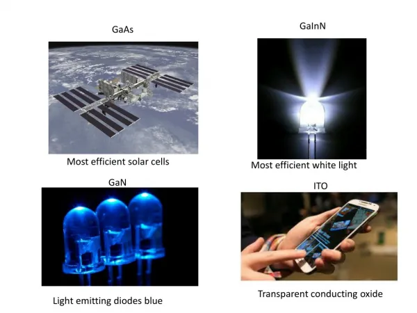
Gallium Arsenide (GaAs) Wafer Market Research Report – Forecast to 2023 Gallium Arsenide (GaAs) Wafer Market Research Report, by Production Method (Vertical Gradient Freeze (VGF), Liquid Encapsulated Czochralski (LEC), Molecular Beam Epitaxy (MBE)), Application (Mobiles, Photovoltaic Devices, Wireless Communication) — Global Forecast till 2023 Market Synopsis Globally, the Gallium Arsenide (GaAs) Wafer Market is expected to grow from USD 625 million in 2017 to USD 1224.3 million by 2023, at a CAGR of 12% during the forecast period. Increasing adoption of 4G and 5G networks drives the Gallium Arsenide (GaAs) Wafer Market. However, the high production cost is restraining the market growth. Gallium Arsenide (GaAs) is a semiconductor compound of two elements gallium (Ga) and arsenic (As). Gallium is a product produced after smelting of aluminum and zinc. GaAs is used in various end-use applications such as solar cells, manufacturing of LEDs, laser diodes, and wireless communication. The GaAs is also used in Field Effect Transistors (FET) and integrated circuits (ICs). In this compound, the velocity of electrons is faster than silicon, which makes it ideal for high velocity and high electric field applications. GaAs is more heat-resistant as compared to silicon which makes it suitable for use in power amplifiers for transmitting high-speed signals. GaAs wafers are suitable for ultra-high radio frequency and fast electronic switching applications. GaAs wafers have many advantages such as better signal to noise ratio, high thermal stability, wider temperature operating range, and high electron mobility. Mobile devices are expected to dominate the application segment during the forecast period. After the launch of 4G and 5G enabled smartphones, the market of 2G and 3G mobile devices dropped significantly, creating opportunities for GaAs market to shift towards 4G and 5G. However, rapid change in new smartphone technologies encourages smartphone manufacturers to replace existing semiconductor wafers. Key players The prominent players in Gallium Arsenide (GaAs) Wafer Market are Advanced Wireless Semiconductor Company (Taiwan), Global Communication Semiconductors, LLC (US), Ommic S.A. (France), WIN Semiconductors Corporation (Taiwan), AXT Inc. (US), Century Epitech Co Ltd. (China), Powerway Advanced Material Co., Ltd. (China), Intelligent Epitaxy Technology, Inc. (US), Sumitomo Electric Semiconductor Materials Inc. (US), Freiberger Compound Materials GmbH (Germany) among others. Other players in GaAs market are IQE plc (UK), Qorvo, Inc. (US), United Monolithic Semiconductors (France), and Visual Photonics Epitaxy Co, Ltd. (Taiwan) among others. Segmentation. By production method, the market is segmented into vertical gradient freeze (VGF), Liquid encapsulated Czochralski (LEC), Molecular Beam Epitaxy (MBE), Metal-Organic Vapor Phase Epitaxy (MOVPE). By application, the market is segmented into mobile devices, photovoltaic devices, wireless communication, optoelectronic devices, aerospace & defense, and others. By region, the market is segmented into North America, Europe, Asia-Pacific and the rest of the world. Regional Analysis The global market for GaAs wafer is estimated to grow at a significant rate during the forecast period from 2018 to 2023. The geographical analysis of Gallium Arsenide (GaAs) Wafer Market is studied for North America, Europe, Asia-Pacific, and the rest of the world. P a g e | 2 Copyright © 2017 Market Research Future.
Gallium Arsenide (GaAs) Wafer Market Research Report – Forecast to 2023 North America is expected to grow at a faster rate during the forecast period due to the presence of major vendors and increasing adoption of new technologies and associated services in the region. Asia-Pacific is expected to dominate the Gallium Arsenide (GaAs) Wafer Market during the forecast period owing to increasing number of smartphone users. Get Report Details @ https://www.marketresearchfuture.com/reports/gaas-wafer-market-6473 Competitive Analysis The Gallium Arsenide (GaAs) Wafer Market has witnessed major trends including growing demand for large size GaAs wafers and reuse of gallium arsenide wafers for high-performance devices. Large GaAs wafers reduce the manufacturing costs by 25-30%. 150 mm wafers are used to manufacture power amplifiers and ICs. The wafer processing industry is moving towards developing 200 mm GaAs wafers to match pace with its biggest competitor — silicon wafers. Regionally, major GaAs suppliers are concentrated in Europe, the US, China, Japan, and Taiwan. MicroLink Devices has achieved a 37.75% power conversion efficiency from a three-junction epitaxial lift-off (ELO) thin-film solar cell. This device’s performance is certified bythe US ‘National Renewable Energy Laboratory’ and tested under AM1.5G industry standard. Intended Audience • Memory chip Manufacturers • Semiconductor Product Manufacturing Companies • Sensors and ICs Manufacturers • Electronic Component Suppliers • Mobile manufacturers • Defense agencies • Telecommunication companies P a g e | 3 Copyright © 2017 Market Research Future.
Gallium Arsenide (GaAs) Wafer Market Research Report – Forecast to 2023 P a g e | 4 Copyright © 2017 Market Research Future.