Download
1 / 1
10 likes | 135 Vues
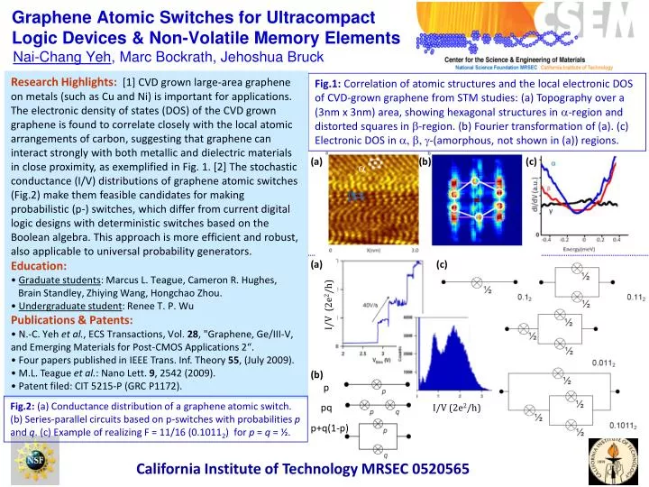
Graphene Atomic Switches for Ultracompact Logic Devices & Non-Volatile Memory Elements Nai-Chang Yeh , Marc Bockrath, Jehoshua Bruck. a. b.

E N D
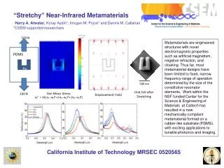
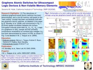
Graphene Atomic Switches for Ultracompact Logic Devices & Non-Volatile Memory Elements Nai-Chang Yeh, Marc Bockrath, Jehoshua Bruck a b • Research Highlights:[1] CVD grown large-area graphene on metals (such as Cu and Ni) is important for applications. The electronic density of states (DOS) of the CVD grown graphene is found to correlate closely with the local atomic arrangements of carbon, suggesting that graphene can interact strongly with both metallic and dielectric materials in close proximity, as exemplified in Fig. 1. [2] The stochastic conductance (I/V) distributions of graphene atomic switches (Fig.2) make them feasible candidates for making probabilistic (p-) switches, which differ from current digital logic designs with deterministic switches based on the Boolean algebra. This approach is more efficient and robust, also applicable to universal probability generators. • Education: • Graduate students: Marcus L. Teague, Cameron R. Hughes, • Brain Standley, Zhiying Wang,Hongchao Zhou. • Undergraduate student: Renee T. P. Wu • Publications & Patents: • N.-C. Yeh et al., ECS Transactions, Vol. 28, "Graphene, Ge/III-V, and Emerging Materials for Post-CMOS Applications 2“. • Four papers published in IEEE Trans. Inf. Theory 55, (July 2009). • M.L. Teague et al.: Nano Lett. 9, 2542 (2009). • Patent filed:CIT 5215-P (GRC P1172). Fig.1: Correlation of atomic structures and the local electronic DOS of CVD-grown graphene from STM studies: (a) Topography over a (3nm x 3nm) area, showing hexagonal structures in a-region and distorted squares in b-region. (b) Fourier transformation of (a). (c) Electronic DOS in a, b, g-(amorphous, not shown in (a)) regions. (a) (b) (c) I/V (2e2/h) (a) (c) p I/V (2e2/h) pq (b) Fig.2: (a) Conductance distribution of a graphene atomic switch. (b) Series-parallel circuits based on p-switches with probabilities p and q. (c) Example of realizing F = 11/16 (0.10112) for p = q = ½. p+q(1-p) California Institute of Technology MRSEC 0520565