Download
1 / 17
170 likes | 230 Vues
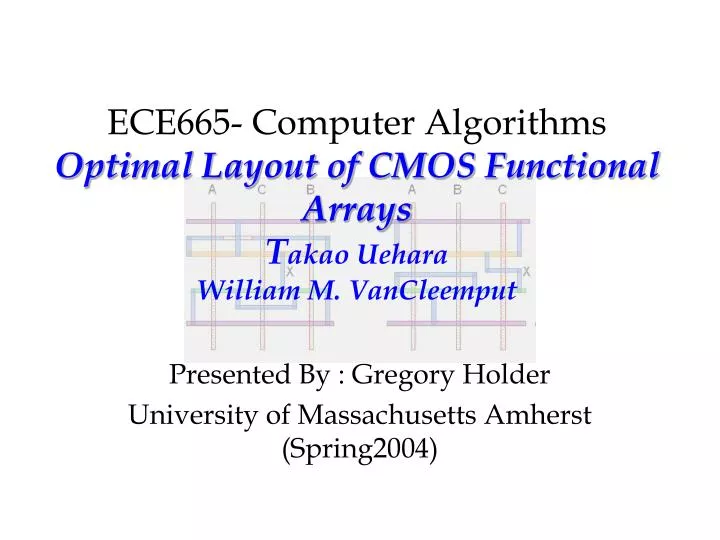
ECE665- Computer Algorithms Optimal Layout of CMOS Functional Arrays T akao Uehara William M. VanCleemput. Presented By : Gregory Holder University of Massachusetts Amherst (Spring2004). Outline:. Weinberger methodology Optimized approach (Sorry Weinberger!) Graph-theoretical algorithm

E N D
ECE665- Computer AlgorithmsOptimal Layout of CMOS Functional ArraysTakao Uehara William M. VanCleemput Presented By : Gregory Holder University of Massachusetts Amherst (Spring2004)
Outline: • Weinberger methodology • Optimized approach (Sorry Weinberger!) • Graph-theoretical algorithm • Heuristics • Conclusion • References Optimal layout of CMOS Functional Arrays
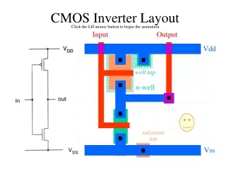
Weinberger methodology • Also called “Weingberger approach” [weinberger67] this method a (structured approach) was traditionally used in the 1980s where the data wires are routed in parallel to the supply rails and perpendicular to the diffusion areas. • This technique was most efficient for bit sliced datapaths, because of the “over the cell wiring”. • Figure 1 on the next slide shows this technique. Optimal layout of CMOS Functional Arrays
Weignberger approach • A more efficient technique has been introduced called the “standard-cell technique”, where signals are now routed vertically and polysilicon can serve for both Nmos and Pmos devices. This has given been the focus of using the Euler Approach. Figure1 • Weinberger (using a single metal layer m1) Optimal layout of CMOS Functional Arrays
Optimized approach (Euler Path) • The Euler path technique has been used in what is called the “standard cell technique”, which results in a dense layout for CMOS gates and one polysilicon strip that can serve as the input to both NMOS and PMOS devices. • Our main aim is to have a single strip of diffusionin both NMOS and PMOS devices. This depends on the “ordering” of the inputs. How do we determine the best order? Figure 2 Optimal layout of CMOS Functional Arrays
Two Versions of C • (A + B)1(Observe the input order) Optimal layout of CMOS Functional Arrays
Graph the theoretical approach • To reduce the size of an array and an uninterrupted diffusion strip we need to find this “Euler path” talked about previously. This is defined as the path through all nodes or vertices (source and drain signals) such that each edge( transistor gate inputs) is only visited exactly once. (vertices maybe visited more than once). • Euler paths are not unique. • Euler paths must be consistent (same ordering in both PUN (pull up network) and PDN (pull down network). • Can Run in linear time3. Optimal layout of CMOS Functional Arrays
Consistent Euler Path1 X PUN A C j C B i VDD X X = C • (A + B) B A j C PDN i A B C A B GND A B C Optimal layout of CMOS Functional Arrays
The General Algorithm • Enumerate all possible decompositions to find the minimum number of Euler paths that cover the graph. • Chain by means of diffusion area according to the order of edges in Euler path. • If more than 2 edges are necessary to cover the graph model, then provide a separation area between each pair of chains. • Therefore for the previous consistent Euler path for the logic structure we achieve the optimal layout below. Figure 3 Optimal layout of CMOS Functional Arrays
Theorem: The following example and any circuit will have a single Euler path if the number of inputs to every AND/OR element is odd. Inaddition, There exist a graph model such that the sequence of edges on an Euler path corresponding to the vertical order of the inputs on a planar representation of the logic diagram. The Heuristic Algorithm To every gate with an even number of inputs add a “pseudo” input. The “pseudo” input does not contribute to separation area. But this input is added so that there is a minimal combination between “pseudo” and real inputs. Construct the graph model according to the vertical order of inputs on logic diagram. Chain together the gates by means of diffusion areas as indicated by the sequence of edges on the Euler path. A “pseudo" input gives a separation between diffusions. Delete “Pesudo” edges in parallel and contacting “pseudo” edges in series with other edges for final circuit. Heuristic Algorithm(of course life not being so easy) Optimal layout of CMOS Functional Arrays
Example We consider the following logic Circuit (a and b), the derived Euler Path (c) and the corresponding Layout. For our Euler path the PUN- and the PDN -----. Optimal layout of CMOS Functional Arrays
Heuristic Works We apply our Heuristic approach to the previous example and we obtain the following sequence (p1,2,3,1,4,5,p2) where we remove the “pseudo” inputs to get the same layout previously shown in slide 11. (Note we choose the combination with the minimum interlaced with real inputs) hence circuit (b). Optimal layout of CMOS Functional Arrays
Analysis • It must be noted that the heuristic algorithm may not always give the optimal layout but if the resulting sequence. However, if no separation areas are obtained then this is the optimal solution. • The heuristic gives excellent results for circuits which do not have a Euler path. This is Illustrated in the four-bit carry look-ahead adder3 circuit shown in this slide. Optimal layout of CMOS Functional Arrays
Analysis (continued) Here in (b) we see the final Euler Path interpretation the corresponding circuit diagram (c) and the a final layout. Optimal layout of CMOS Functional Arrays
Conclusion • This Presentation has given a brief incite into optimizing the layout of complex CMOS gates. Using the Euler path approach and a heuristic algorithm. The results show that by use of this approach we can optimize considerably on area in our layout. Further work can be done to simulate the “real” gain of this method in terms of power and performance of a particular design. Optimal layout of CMOS Functional Arrays
References • Digital integrated circuits 2nd edition • Uehara, T. and Vancleemput, W. M “optimal layout of CMOS Functional Arrays”. • Robert Sedgewick “Algorithms in C third edition”. • Forbes, B. E. “Silicon-on Sapphire Technology Produces High-Speed Single- Chip Processor, “Hewlett-Packard Journal, April 1977,pp 2-8. Optimal layout of CMOS Functional Arrays
Thanks To ALL Optimal layout of CMOS Functional Arrays