Download
1 / 21
210 likes | 310 Vues
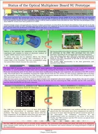
On the development of the final optical multiplexer board prototype for the TileCal experiment. V. González Dep. of Electronic Engineering University of Valencia, Spain. Outline. Introduction Previous work OMB 6U Final prototype OMB 9U Present status. Introduction.

E N D
On the development of the final optical multiplexer board prototype for the TileCal experiment V. González Dep. of Electronic Engineering University of Valencia, Spain
Outline • Introduction • Previous work OMB 6U • Final prototype OMB 9U • Present status
Introduction • RODs interface LVL1 and LVL2 at each detector • Some preprocessing available if needed • For TileCal, radiation issues changed front end connection to RODs • Two fibers with same data output each FrontEnd board • Need to select the fiber with good data in case of errors (OMB aka PreROD)
Previous work OMB 6U • Specifications • VME 6U Board format • 2 input channels (4 input fibers) @ 640 Mbit/s • 2 output channels (2 output fibers) • Digital data analysis (CRC computation) • Trigger and Busy inputs
Previous work OMB 6U • Functionality • Error detection (multiplexing) • Data injection • Preconfigured event (counter) • Configurable event loadable through VME • Different trigger options • External (NIM or LVTTL) • Internal. Variable frequency • Single • Loop • Non-stop
Previous work OMB 6U • Designed with Cadence PSD 15.0 and Altera Quartus II for FPGA programs • Technical details • 2 Cyclone EP1C12 and 1 ACEX EP1K100 FPGAs • 12 copper layers, 35 μm thick • > 2000 routes 0.15 mm width • > 2000 vias 0.2 mm • SMD components widely used
Previous work OMB 6U • TEST at Valencia LAB • Firmware adjustment • Integration with ROD motherboard • Development of control software (XTestROD) • TEST at CERN (USA15) • During commissioning • Integration with 8 TileCal ROD • Used now for ROD production tasks
Final prototype OMB 9U • Same basic functionality • CRC checking • Data injection • 40 MHz clock • Differences • 8 channels • 16 input fibers • 8 output fibers • TTCrx • Mezzanine connectors: more processing power?
Final prototype OMB 9U • Technical details • 9U VME slave board • Dual optoelectronic transmitter/receiver (Stratos) • GLINK chips • 8 HDMP-1032: transmitter • 16 HDMP-1034: receiver • 8 Cyclone EP1C12 (CRC FPGA) • One for each channel (2 input fibers and 1 output fiber) • 1 Cyclone EP1C20 (VME FPGA) • Changed from ACEX in 6U version for more logic resources • Includes TTCrx control firmware
Final prototype OMB 9U • PCB details • Input/output signals designed for operation at 80 MHz • 10 copper layers • Signal layers between power/gnd planes • Adjacent layers routed orthogonally for minimum coupling
Final prototype OMB 9U • Signal integrity issues • Big area, not too much populated • Long distance traces (high coupling) • Clock distribution • JTAG chain distribution • VME-CRC FPGA serial bus • Different voltage supplies • +3.3 Volt for FPGA I/O and some logic • +1.5 Volt for FPGA cores (island) • +5 Volt for logic • +12 Volt for NIM/TTL conversion (ext. trigger input)
Final prototype OMB 9U • Example of SI analysis: VME to CRC serial BUS • Connected between the VME FPGA and all CRC FPGAs • For control, communication, configuration, etc. • 4 lines: CLK, DATA0, DATA1, DATA2, DATA3 • Frequency of operation 40 MHz
Final prototype OMB 9U • First attempt • Manual placement and routing of bus lines • Keep stubs short • Keep same routing layer as much as possible • R, RC termination • Problem • Characteristic impedance change at T junction • Reflections at first FPGA creates InterSymbol Interference (ISI)
Final prototype OMB 9U • PostLayout simulation
Final prototype OMB 9U • Second attempt • Manual placement and routing of bus lines • Keep stubs short • Keep same routing layer as much as possible • Problem • Reflections with different termination schemes
Final prototype OMB 9U • PostLayout simulation
Final prototype OMB 9U • Final attempt • Manual placement and routing of bus lines • Keep stubs short • Keep same routing layer as much as possible • Solution • Resistive termination at both ends
Final prototype OMB 9U • PostLayout simulation
Present status • Stratos change connectors to be RoHS compliant • Need to test new connectors • Board routing on the way • SI analysis still undergoing: JTAG chain, clock distribution and power distribution • FPGA firmware adaptation