VLSI Projects
ClickMyProject is the leading center in Madurai offering IEEE, online, and readymade VLSI Projects in engineering and computer science domains for students seeking innovative VLSI project solutions.


VLSI Projects
E N D
Presentation Transcript
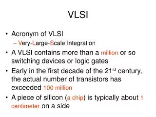
The modern digital world is inextricably linked to silicon. From the high-performance computing centers powering generative AI to the minute, low-power sensors driving the vast network of the Internet of Things (IoT), every significant technological advancement is fundamentally enabled by Very Large Scale Integration (VLSI). This sophisticated engineering discipline is responsible for consolidating billions of transistors onto a single die, creating the complex silicon chips that form the very core of contemporary devices. The creation of these powerful integrated circuits (ICs) is the ultimate objective of successful VLSI Projects, which constantly push the boundaries of speed, efficiency, and scale in electronics. For students, aspiring engineers, and career researchers, practical involvement in VLSI Projects is not merely supplementary—it is the single most critical pathway for transitioning from abstract theoretical knowledge to tangible, industry-ready expertise. VLSI design requires a unique synthesis of knowledge across computer architecture, logic design, semiconductor physics, and rigorous verification methodologies. By engaging in hands-on VLSI Projects, individuals master the essential workflow of the semiconductor industry, learning to navigate the critical trade-offs in Power, Performance, and Area (PPA) that define a commercially viable chip. This comprehensive guide serves as your definitive roadmap to navigating the complexities of the field. We will delve deeply into every essential facet of VLSI Projects, starting with foundational concepts and indispensable EDA toolchains. We will then transition into advanced topics, exploring state-of-the-art design methodologies, the crucial importance of verification, and the best practices for project execution. Finally, we will inspire your next endeavor with cutting-edge VLSI Project ideas that align with modern trends in AI, hardware security, and low-power design, ensuring you are equipped to build the future, one chip at a time. The Foundational Landscape of VLSI Projects VLSI is the process of creating integrated circuits (ICs) by combining millions or now, billions of transistors onto a single chip. It is the technological bedrock that powers modern life. VLSI Projects are essentially the development and implementation of a functional electronic system using this technology, often culminating in an ASIC (Application-Specific Integrated Circuit) or an FPGA (Field-Programmable Gate Array) implementation. What Defines a Successful VLSI Project? A successful VLSI Project is characterized by meeting its specified functional requirements while adhering to crucial non-functional constraints, often referred to as PPA: Power: Minimizing the energy consumption of the chip. This is critical for mobile and IoT applications. Performance: Achieving the required operating frequency (speed) and throughput. Area:Optimizing the chip’s physical size, which directly impacts manufacturing cost. Every VLSI Project, regardless of its complexity, must balance these three competing factors. The challenge in sophisticated VLSI Projects lies in finding the optimal trade-off.
The Two Pillars of VLSI Projects: Front- End and Back-End VLSI Projects are organized into two major phases, each requiring distinct skills and tools: 1. Front-End Design (Logic and Behavioral Design): 1. Objective:To define the circuit’s function and behavior. 2. Key Tasks: System specification, architectural design, coding using Hardware Description Languages (HDLs) like Verilog or VHDL, and extensive functional verification. 3. Output: A verified RTL (Register Transfer Level) netlist. Many entry-level VLSI Projects focus heavily on this stage. 2. Back-End Design (Physical Design): 1. Objective: To translate the functional design into a physical layout suitable for fabrication. 2. Key Tasks: Synthesis (converting RTL to a gate-level netlist), floor planning, power planning, placement, Clock Tree Synthesis (CTS), routing, and final timing and physical verification (DRC/LVS). VLSI Projects in this area require deep knowledge of semiconductor physics and fabrication processes. 3. Output: The GDSII file (Graphical Data System II), which is the final blueprint for the manufacturing foundry. Understanding this division is the first step in scoping any complex VLSI Project. Essential Tool chain for VLSI Projects No VLSI Project can be completed without a robust Electronic Design Automation (EDA) tool chain. These software suites automate the painstaking and complex tasks of chip design and verification. Familiarity with these tools is crucial for anyone engaging in serious VLSI Projects.
Tool Category Function in VLSI Projects Example Software ModelSim/QuestaSim, Icarus Verilog Writing, compiling, and functionally verifying the HDL code. HDL and Simulation Synopsys Design Compiler, Cadence Genus Converting the HDL code into a gate-level netlist based on a specific technology library. Synthesis Synopsys IC Compiler II, Cadence Innovus Physical Design (P&R) Performing placement, routing, and optimization for timing and power. Static Timing Analysis (STA) Analyzing all paths in the circuit to ensure timing constraints are met. Synopsys PrimeTime FPGA Implementation Mapping, fitting, and generating the bitstream for the target FPGA. Xilinx Vivado, Intel Quartus Prime Categorizing and Ideating Advanced VLSI Projects The scope for VLSI Projects is virtually limitless, spanning every sector of modern technology. A focused approach is key to selecting a manageable yet impactful project. 1. FPGA-Based VLSI Projects: Rapid Prototyping
FPGA projects are ideal for beginners and for applications requiring high parallelism and quick turnaround. They allow a designer to implement and test a complex digital system in a matter of hours or days. Digital Signal Processing (DSP) VLSI Projects: o Implementation of advanced Finite Impulse Response (FIR) or Infinite Impulse Response (IIR) filters with high-throughput architecture. o Fast Fourier Transform (FFT) Accelerator: Designing a highly pipelined and parallel architecture for real-time spectral analysis, a core component in many communication and audio VLSI Projects. Image and Video Processing VLSI Projects: o Edge Detection Accelerator: Implementing Canny or Sobel edge detection algorithms in hardware for real-time processing of video streams. o Image Compression/Decompression: Implementing a simplified JPEG or MPEG encoder/decoder. These VLSI Projects demand careful use of on-chip block RAM and DSP slices. Communication Protocol VLSI Projects: o Designing and verifying a hardware implementation of a standard protocol like SPI, I2C, UART, or a more complex one like Ethernet MAC (Media Access Control) or PCIe endpoint. 2. ASIC-Focused VLSI Projects: The Power-Performance Nexus ASIC projects are more complex and typically involve the full front-to-back design flow, aiming for optimized performance and low power, often targeting specific application needs. While full fabrication is often too costly for academic VLSI Projects, the full design flow up to the GDSII file can be simulated. Custom Processor Core VLSI Projects: o RISC-V Microprocessor Implementation: Designing a simple 3-stage or 5-stage pipelined RISC-V core. This is one of the most intellectually rewarding VLSI Projects as it involves all aspects of computer architecture. o Hardware Accelerator for Specific Tasks: Creating a dedicated hardware unit (e.g., a custom instruction) to speed up an operation like matrix multiplication or encryption (AES/SHA). Low-Power VLSI Projects: o Implementation of dynamic power management techniques like Multi-Voltage Design or Dynamic Voltage and Frequency Scaling (DVFS) in a test module. o Exploring advanced logic styles like Adiabatic Logic for ultra-low energy consumption in specialized applications. Low-power constraints define a crucial subset of contemporary VLSI Projects. 3. Cutting-Edge VLSI Projects: Addressing Modern Challenges Modern VLSI Projects are increasingly focused on enabling Artificial Intelligence and Internet of Things (IoT) applications. AI/ML Accelerator VLSI Projects: o Neural Network Inference Engine: Designing a hardware architecture optimized for performing the weighted sum and activation function of a small Convolutional Neural Network (CNN) or a simple Multi-Layer Perceptron (MLP). This involves optimizing data flow and parallelism. o Systolic Array Design: Implementing a systolic array for highly efficient matrix multiplication, a fundamental operation in deep learning. These are state-of-the-art VLSI Projects. Security VLSI Projects: o True Random Number Generator (TRNG) Design: Implementing a TRNG based on physical noise sources for cryptographic applications. o Physical Unclonable Function (PUF) Implementation: Designing a circuit that derives a unique chip ID from random manufacturing variations, often based on SRAM cells or ring oscillators. Security-focused VLSI Projects are increasingly critical in the connected world. IoT and Mixed-Signal VLSI Projects:
o Designing a simplified Sensor Interface Hub that includes digital filtering, a simple state machine, and a mechanism for data packetization. The Execution Pipeline for Successful VLSI Projects Executing a large-scale VLSI Project requires meticulous planning and adherence to a strict workflow. This disciplined approach ensures that errors are caught early, where they are cheapest and easiest to fix. Phase 1: Specification and Requirements The most critical step in any VLSI Project is defining what the chip needs to do. This phase establishes the “why”and “what.” System Requirements:Defining the functionality (e.g., “Must sort 1024 numbers”). Performance Requirements:Specifying the speed (e.g., “Must run at 500 MHz”) and latency. Interface Requirements: Detailing how the design connects to the outside world (e.g., “Uses an AXI4-Lite interface for configuration”). Test Plan: Crucially, a good VLSI Project begins with a clear plan for how the final design will be tested and verified. Phase 2: HDL Coding and Modularization With specifications in hand, the design is translated into an HDL. For complex VLSI Projects, a modular approach is essential. The overall system is broken down into smaller, manageable sub- blocks (e.g., arithmetic unit, control unit, register file). Coding Style: Adopting a clean, synchronous coding style is paramount. All data path elements should be registered, and asynchronous logic should be minimized or strictly isolated. Good coding practices significantly simplify later stages of the VLSI Project. Parameterization: Using parameters in Verilog/VHDL allows the design to be easily reconfigured for different bit-widths, block sizes, or pipeline stages, making the VLSI Project more reusable. Phase 3: Verification – The Core of VLSI Projects The reality in the industry is that verification consumes 60-80% of the total effort for most VLSI Projects. A design is useless if it is not provably correct. Testbenches: Creating robust test environments (testbenches) is essential. Simple testbenches might use directed tests (specific input patterns), while advanced VLSI Projects use constrained random verification (CRV) to explore corner cases that human designers might miss. Coverage: Verification engineers track coverage metrics: o Code Coverage: Ensuring every line, branch, and condition in the HDL code has been executed. o Functional Coverage: Ensuring every critical operation defined in the specification has been tested. Formal Verification: For smaller, mission-critical blocks (like a FIFO controller), formal methods can mathematically prove the absence of certain bugs, providing an extremely high level of confidence in the VLSI Project’s correctness. Phase 4: Synthesis and Logic Optimization Synthesis is the automated process of converting the abstract RTL code into a gate-level netlist, using specific gates available in the target technology library
Timing Constraints: The designer must provide the synthesis tool with accurate timing constraints (Syllable Design Constraints – SDC). These constraints tell the tool the required clock frequency, input arrival times, and output required times. Optimization: The synthesis tool optimizes the netlist for PPA. It may restructure logic, perform gate sizing, or insert buffers to meet the specified timing goals of the VLSI Project. Phase 5: Physical Implementation (The Back-End) This phase turns the logical netlist into a physical layout. Floor Planning:Deciding the placement of major blocks (e.g., memory, I/O pads) on the chip’s floor. This initial step critically impacts the routability and timing of the final VLSI Project. Clock Tree Synthesis (CTS): The clock signal must arrive at every register simultaneously (or with controlled skew). CTS builds a balanced network of buffers to minimize clock skew, a major challenge in high-speed VLSI Projects. Routing: Connecting the billions of wires (nets) between the gates, respecting design rules (spacing, width). Post-Layout Verification: After routing, parasitic extraction is performed, generating a detailed netlist including the resistance and capacitance of the wires. This is fed back into STA to perform a final, accurate check on the timing. This is the final sign-off for the VLSI Project. Challenges and Best Practices for VLSI Projects The complexity of modern chip design means that VLSI Projects inevitably face significant challenges. Proactive strategies are required to mitigate these risks. The Power Challenge in VLSI Projects Power dissipation is arguably the single biggest limiting factor in modern designs, especially in mobile and data center applications. Leakage Power:The static current that flows even when the transistor is “off.” This dominates power consumption in advanced sub-micron technologies. Low-power VLSI Projects often focus on using multiple threshold voltages (MTCMOS) to manage leakage.
Dynamic Power: Power consumed when transistors switch states. Solutions include Clock Gating (turning off the clock to idle blocks) and Data Gating (preventing unnecessary data changes), which are crucial optimizations in any high-efficiency VLSI Project. The Timing Closure Challenge Achieving timing closure ensuring that all data arrives at the destination register before the clock edgecan be the most time-consuming task. Critical Path Management: The longest delay path is the critical path. Identifying and shortening this path (through pipelining, logic restructuring, or judicious placement/routing) is central to completing high-speed VLSI Projects. Iteration and Flow: Timing closure is iterative. Designers often must go back from the back-end (physical layout) to the front-end (RTL) to make architectural changes if the timing cannot be met, demonstrating the interconnected nature of every step in VLSI Projects. Best Practices for Selecting and Executing VLSI Projects 1. Start Small and Master the Fundamentals: A successful first VLSI Project should focus on mastering a single tool or concept (e.g., a simple synchronous FIFO, a basic processor instruction). Incremental complexity is key. 2. Verify First, Code Later: Always write the test plan before writing the RTL code. This ensures the design meets the required functionality and forces a complete understanding of the specification. This principle is vital for robust VLSI Projects. 3. Choose Open Source and Standards: Leveraging open-source hardware (like RISC-V or OpenCores) for initial blocks can accelerate the learning curve and allow the VLSI Project team to focus on innovation rather than re-implementing standard, non-differentiating components. 4. Documentation is Not Optional: Thorough documentation of the architecture, design choices, and verification results is essential for any professional VLSI Project and facilitates debugging. Frequently Asked Questions 1. What is the difference between an FPGA and an ASIC in the context of VLSI Projects? An FPGA (Field-Programmable Gate Array) is a pre-fabricated chip whose internal logic blocks and interconnections can be configured by the user after manufacturing. FPGA-based VLSI Projects are fast to develop, ideal for prototyping, and flexible. An ASIC (Application-Specific Integrated Circuit) is designed from scratch for a single purpose. ASIC VLSI Projects are expensive to develop but offer superior PPA (Power, Performance, Area) once mass-produced because the design is fully optimized for the intended function. 2. Is programming knowledge in Python or C++ necessary for VLSI Projects? Yes, increasingly so. While VLSI Projects are primarily implemented using Hardware Description Languages (Verilog/VHDL), verification often uses SystemVerilog or UVM (Universal Verification Methodology). The testbenches and associated scripts for automation, regression testing, and data analysis are almost universally written in Python or occasionally Perl. Understanding data structures and object-oriented programming is a major asset in modern VLSI Projects. 3. What are some of the most sought-after skills for VLSI Projects in the industry? The most in-demand skills revolve around verification and physical design: 1. Advanced Verification Methodologies: SystemVerilog and UVM. 2. Timing Closure and STA: Expertise in Synopsys PrimeTime and meeting aggressive clock constraints. 3. Physical Design Automation: Scripting skills for layout, placement, and routing (P&R). 4. Low-Power Design Techniques: Applying clock gating, power gating, and DVFS techniques. These are core competencies for tackling complex VLSI Projects.
4. How can I practice VLSI projects without access to expensive EDA tools through ClickMyProject? ClickMyProject supports students who want to work on VLSI projects even without costly professional software. We guide learners to use free and open source environments such as Icarus Verilog for simulation and Yosys for synthesis. For layout design, we help students practice using the SkyWater 130nm PDK along with tools like Magic, enabling a complete back end design flow. These accessible platforms make it easier for beginners to gain strong VLSI skills without financial limitations. 5. What role does hardware software co design play in modern VLSI projects at ClickMyProject? ClickMyProject emphasizes hardware software co design as a key part of advanced VLSI development. In our project guidance, we help students understand how to divide system tasks so that performance intensive operations run on custom hardware modules while the remaining logic is handled efficiently by software on a CPU core. This balanced approach ensures high speed processing and optimized system behavior for modern applications including embedded systems and artificial intelligence. The Future is Built on VLSI Projects The landscape of technology is continually being reshaped by the innovation derived from VLSI Projects. From the high-performance computing centers powering the next generation of AI to the tiny, ultra-low-power sensors enabling the vast network of the IoT, every advance is an achievement in silicon design. Undertaking VLSI Projects offers an unparalleled opportunity to master a multidisciplinary field that combines logic design, computer architecture, programming, and semiconductor physics. The complexity is immense, but the reward—the ability to design and build the fundamental components of the digital age is transformative. By meticulously following the design flow, embracing rigorous verification, and focusing on the crucial PPA metrics, aspiring engineers can turn their theoretical knowledge into tangible, industry-ready chips. The next generation of technological breakthroughs is waiting to be integrated into reality through powerful and efficient VLSI Projects.