Download

1 / 3
0 likes | 11 Vues
semiconductor epi wafer manufacturing market

E N D
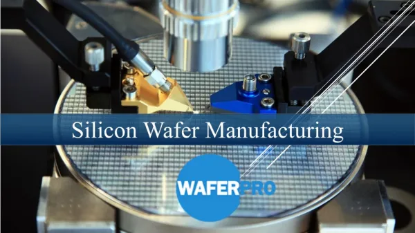
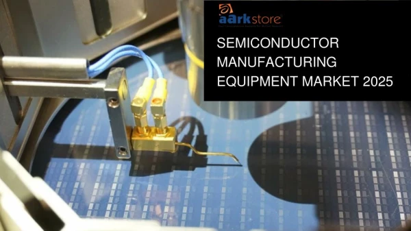
+1 217 636 3356 +44 20 3289 9440 sales@mobilityforesights.com Your Cart 0 Company Market Reports Consumer Research Advisory Services Exports - Imports Careers Contact Us Blog Your cart is empty Your Name Return to Shop Business Email Global Semiconductor EPI Wafer Manufacturing Market 2024-2030 Country Phone Number +1 Company Name Single User License : $ 4,000 Your message Corporate User License : $ 6,000 By submitting this form, you are agreeing to Request Sample the Terms of Use and Privacy Policy. I'm not a robot reCAPTCHA Privacy - Terms BUY NOW DOWNLOAD SAMPLE DESCRIPTION TABLE OF CONTENTS SEMICONDUCTOR EPI WAFER MANUFACTURING MARKET INTRODUCTION An epitaxial wafer is a semiconducting wafer grown epitaxially for application in photonics, microelectronics, spintronics, or photovoltaics. The epi layer can be made of the same material as the substrate, which is commonly monocrystalline silicon, or it can be made of silicon dioxide (Soi) or a more exotic material with certain desired properties. The goal of epitaxy is to perfect the crystal structure over the bare substrate beneath and enhance the electrical properties of the wafer surface, making it suitable for extremely complicated microprocessors and memory devices. When the epi-layer and substrate are made of the same material, ion implantation is used to deposit a thin layer of crystal impurity atoms and the associated mechanical stress at the precise depth of the desired epi layer thickness. In the ensuing cleavage stage, the resultant localized stress offers a controlled channel for fracture growth. A controlled crack is driven by a temperature change at the epi/wafer interface purely by thermal stresses due to the mismatch in thermal expansion between the epi layer and substrate in the dry stress lift-off process. This is applicable when the epi-layer and substrate are suitably different materials, without the need for any external mechanical force or tool to aid crack propagation. This technique was reported to produce single atomic plane cleavage, minimizing the requirement for post-lift-off polishing and allowing up to ten substrate reuses. Silicon epitaxy is the technique of depositing an extra monocrystalline silicon layer on the polished crystal surface of a silicon wafer. This procedure allows for the selection of material qualities independent of the polished substrate, resulting in wafers with varied properties in the substrate and the epitaxial layer. 0 In many circumstances, this is required for the semiconductor component to perform properly. The epitaxial layers may be composed of compounds with favorable properties such as gallium nitride (Gan), gallium arsenide (GaAs), or a mixture of Continue Shopping gallium, indium, aluminum, nitrogen, phosphorus, or arsenic. Because the thermal expansion coefficients of silicon and Gan are so dissimilar, Gan epitaxy necessitates the formation of a buffer layer on the polished silicon wafer first. Mechanical tension between the two materials can therefore be reduced. Furthermore, an Alga layer is formed on top of the Gan layer to generate a two-dimensional electron plasma at the interface of these two layers. Electrons may travel at very high speeds at the device level, making Gan superior to traditional silicon technology. EPI stands for Epitaxial Growth. It is a process of growing a thin layer of semiconductor material on top of a substrate. The substrate is typically a silicon wafer, but other materials can also be used. The epitaxial layer can be of a different material than the substrate, or it can be the same material with different doping levels. EPI wafer manufacturing is a complex process that involves several steps. The first step is to clean the substrate. This is done to remove any contaminants that could interfere with the growth of the epitaxial layer. The substrate is then heated to a high temperature and a gas containing the desired semiconductor material is introduced. The gas reacts with the substrate and forms a thin layer of semiconductor material. The thickness of the layer can be controlled by the amount of time that the gas is exposed to the substrate. Once the epitaxial layer has been grown, it is cooled and then processed further. This may include ion implantation, doping, and annealing. The final step is to test the wafer to make sure that it meets the desired specifications. EPI wafer manufacturing is a critical process in the production of semiconductors. It is used to create a variety of semiconductor devices, including integrated circuits, transistors, and diodes. SEMICONDUCTOR EPI WAFER MANUFACTURING MARKET SIZE AND FORECAST
+1 By submitting this form, you are agreeing to the Terms of Use and Privacy Policy. The Global Semiconductor Epi Wafer Manufacturing Market accounted for $XX Billion in 2023 and is anticipated to reach $XX Billion by 2030, registering a CAGR of XX% from 2024 to 2030. SEMICONDUCTOR EPI WAFER MANUFACTURING MARKET LAUNCH Resonate Corporation has begun mass production of a third generation of high-grade silicon carbide (Sic) epitaxial wafer (HGE-3G) for power semiconductors. HGE-3G has a higher quality than second-generation high-grade Sic epi-wafer (HGE- 2G), which has been mass-produced up to now. Sic power semiconductor lowers power loss during electricity conversion and emits less heat than conventional silicon-wafer- based power semiconductor, saving energy. As a result, demand for Sic power semiconductors is fast expanding, particularly in industrial applications such as electric vehicles (EVs) and renewable-energy-based power production. Sic epi-wafers are created by depositing and growing an epitaxial Sic layer on the surface of a single crystal Sic substrate, and they are utilized as the primary material for Sic power. As the world’s biggest independent provider of world-class Sic epi- wafers, Resonance is well-regarded by numerous device makers. High-end versions of power semiconductors for use in high-priced EVs and railcars must transmit higher-density electric current to achieve high output while preserving space. To achieve high-density electric current conduction, Sic-epi-wafer producers must develop technology to avoid the growth of dislocation faults in the Sic substrate into the epitaxial Sic layer. This time, Resonance created cutting-edge technology to generate epitaxial Sic layers, effectively resolving the aforementioned issue, and began mass-producing third-generation high-grade Sic epi-wafers. This HGE-3G offers outstanding reliability under high electric current density and will help Sic-based high-end power modules expand. Showa Denko K.K. (SDK) will introduce the biggest size silicon carbide (Sic) epitaxial wafers currently available on the global market for usage in power devices. Next month, the business will also begin offering Sic epitaxial wafers with fewer flaws and more uniformity. SDK has previously produced and sold Sic epitaxial wafers. Furthermore, SDK has worked to build next-generation Sic epitaxial wafers, which will lead to greater productivity, and has provided samples. The firm has planned to commence commercial shipments as soon as the volume manufacturing technology has been established and the product requirements have been finalized. SDK will continue its efforts to improve product quality and boost manufacturing capacity following the development of product lines. THIS SEMICONDUCTOR EPI WAFER MANUFACTURING MARKET REPORT WILL ANSWER FOLLOWING QUESTIONS 1. How many Semiconductor EPI Wafer Manufacturing are manufactured per annum globally? Who are the sub- component suppliers in different regions? 2. Cost breakup of a Global Semiconductor EPI Wafer Manufacturing and key vendor selection criteria 3. Where is the Semiconductor EPI Wafer Manufacturing manufactured? What is the average margin per unit? 4. Market share of Global Semiconductor EPI Wafer Manufacturing market manufacturers and their upcoming products 5. Cost advantage for OEMs who manufacture Global Semiconductor EPI Wafer Manufacturing in-house 6. 5 key predictions for next 5 years in Global Semiconductor EPI Wafer Manufacturing market 7. Average B-2-B Semiconductor EPI Wafer Manufacturing market price in all segments 8. Latest trends in Semiconductor EPI Wafer Manufacturing market, by every market segment 9. The market size (both volume and value) of the Semiconductor EPI Wafer Manufacturing market in 2024-2030 and every year in between? 10. Production breakup of Semiconductor EPI Wafer Manufacturing market, by suppliers and their OEM relationship RELATED REPORTS Global LED Strip Lights Market 2022-2027 India Gas Sensor Market 2022-2027 Global Thickness Sensor Market 2022-2027 India Chemical Sensor Market 2022-2027
$4,000 $4,000 $4,000 $4,000 Multi User Multi User Multi User Multi User License - License - License - License - MARKET REPORTS CONSUMER RESEARCH INFORMATION ADVISORY SERVICES CONTACT INFORMATION 172/1, 2nd Floor, 5th Main, 9th Cross Automotive and Transportation About Us Focus Group Study Transaction Advisory Rd, Opposite to Kairalee Nikethan Semiconductor Our Clientele +1 Education Trust, Indira Nagar 1st Stage, Ethnographic Market Positioning Agriculture and Construction Our People Bengaluru, Karnataka 560038, INDIA Research Assessment Equipment Blog Brand Awareness Custom Automotive Aerospace and Defense +1 217 636 3356, +44 20 3289 9440 Contact us Study Market Research Marine and Rail Terms & Conditions sales@mobilityforesights.com By submitting this form, you are agreeing to Consumer Satisfaction Strategic Advisory Logistics and Packaging Privacy Policy the Terms of Use and Privacy Policy. Survey Competitive Working Hours: Mon - Fri (9 AM - 9 PM Medical Devices ESOMAR Guidelines Consumer Expectation Intelligence IST) Chemical and Materials Compliant & Loyalty Assessment Electrical Machinery Connect with us ICT Energy, Power and Robotics New Technologies © Copyright 2017-2023. Mobility Foresights. All Rights Reserved.