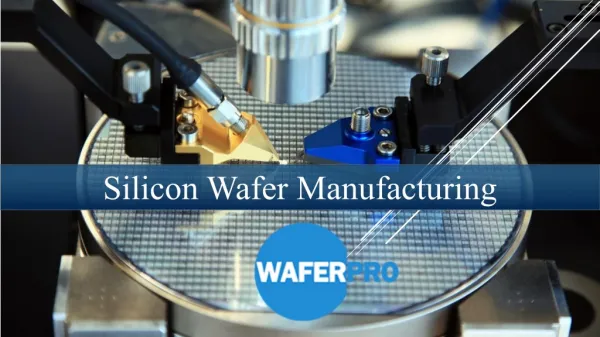
Wafer Manufacturing
Wafer Manufacturing. Farshid Karbassian. Outline. Semiconductor Materials Purification Crystal pulling Czochralski Float-Zone Grinding Slicing. Outline. Edge Rounding Lapping Etching Chemical Mechanical Polishing (CMP) Epitaxial Deposition. Semiconductor Materials. Elemental


Wafer Manufacturing
E N D
Presentation Transcript
WaferManufacturing FarshidKarbassian
Outline • Semiconductor Materials • Purification • Crystal pulling • Czochralski • Float-Zone • Grinding • Slicing
Outline • Edge Rounding • Lapping • Etching • Chemical Mechanical Polishing (CMP) • Epitaxial Deposition
Semiconductor Materials • Elemental Si, Ge • Binary Compounds IV-IV SiC III-V AlP, AlAs, AlSb, GaN, GaP, GaAs, GaSb, InP, InAs, InSb II-VI ZnO, ZnS, ZnSe, ZnTe, CdS, CdSe, CdTe, HgS IV-VI PbS,PbSe,PbTe
Semiconductor Materials • Ternary Compound AlxGa1-x As, AlxIn1-x As, GaAs1-xPx , GaxIn1-x As, GaxIn1-xP • Quaternary Compound AlxGa1-x As1-ySby , GaxIn1-x As1-yPy
Purification Wafer Lapping and Edge Grind Crystal Growth Cleaning Shaping Etching Inspection Wafer Slicing Polishing Packaging Basic Process Steps
Polysilicon Seed crystal Crucible Heater Polishing head Slurry Polishing table 1. Crystal Growth 2. Single Crystal Ingot 3. Crystal Trimming and Diameter Grind 4. Flat Grinding 5. Wafer Slicing 6. Edge Rounding 7. Lapping 8. Wafer Etching 9. Polishing 10. Wafer Inspection
Purification of Silicon Common quartz sand is mainly silicon dioxide, which can react with carbon at high temperatures. Carbon used doesn't need very high purity; it can be in the form of coal, coke or even pieces of wood. At a high temperature carbon starts to react with SiO2 to form carbon mono or dioxide.
Purification of Silicon • This process generates polysilicon with about 98% to 99% purity called crude silicon or MGS. • MGS has high impurities that makes it inconvenient for electronic applications. • To purify MGS, the crude silicon is ground into fine powder. Then the powder is introduced into a reactor to react with HCl vapor, forming any of a number of SiHCl. MGS: Metallurgical-Grade Silicon
Purification of Silicon • The chemical reaction can be expressed as: • TCS (SiHCl3) vapor then goes through a series of filters, condensers and purifiers to get ultrahigh-purity liquid TCS. (9s!) • TCS now has less than one impurity per billion atoms.
Purification of Silicon • Purified polysilicon is obtained from TCS which is purified earlier by fractional distillation, in a large CVD reactor. • The high purity polysilicon is called electronic-grade silicon, or EGS.
Crystal Pulling • The EGS which is obtained from CVD has polycrystalline structure whereas Si which is used in fabrication of electronic devices is single crystal. • The resulting polysilicon may be broken up into pieces to load into crucibles for Czochralski crystal growth or the poly rod itself could be used as the starting material for float-zone crystal growth.
Crystal Pulling (cont.) • Crystallization methods: • Czochralski (CZ) • Float-zone (FZ)
Czochralski Crystal Growth • During CZ crystal growth, the seed and the crucible are normally rotated in opposite directions to promote mixing the liquid and more uniform growth.
Czochralski Crystal Growth Why CZ is much more common? • The CZ process is cheaper. • It is capable of producing large diameter crystals, from which large diameter wafers can be cut.
88 die 200-mm wafer 232 die 300-mm wafer Czochralski Crystal Growth Assume 1.5x1.5 cm2 microprocessor
Czochralski Crystal Growth • The only significant drawback to the CZ method is that the silicon is contained in liquid form in a crucible during growth and as a result, impurities from the crucible are incorporated in the growing crystal.
Czochralski Crystal Growth • Oxygen and carbon are the most significant contaminants. • To avoid additional impurities from the ambient, the growth is normally performed in an argon ambient.
RF Float-Zone (cont.) Gas inlet (inert) Chuck Polycrystalline rod (silicon) Molten zone Traveling RF coil Seed crystal Chuck Inert gas out
Float-Zone • Not to use any crucible in the FZ method impurity levels particularly oxygen is much lowered in the resulting crystal. And it makes easier to grow high-resistivity material. Thus the FZ process is used when only high resistivity, low oxygen content or both is required.
Grinding • The boule is placed in a lathelike machine to grind with a diamond wheel into a perfect cylinder. • After the boule is ground to an appropriate diameter one or more “flats” are normally ground along its length.
Preparing crystal ingot for grinding Internal diameter wafer saw Diameter grind Flat grind Grinding
Slicing • The boule is sliced into individual wafers by a rapid-rotating, inward-diameter diamond-coated saw which cuts on its inside edge.
Edge Rounding • After sawing, preventing the wafer chipping during the mechanical handling, the wafer edge is ground in a mechanical process to round the sharp edges created in the slicing process.
Lapping • The lapping operation is done under pressure using a mixture of alumina (Al2O3), water and glycerine to improve the flatness of the wafer to about ±2 µm, removing most of the taper and bow that results from the sawing operation. • This process removes about 50 µm from both sides of the wafer
Etching • To remove any particles and damages that many still remain from sawing and lapping steps chemical etching is done as a batch process, with the wafers are loaded into cassettes and immersed in a mixture of nitric, hydrofluoric and acetic acids.
Upper polishing pad Wafer Slurry Lower polishing pad Chemical Mechanical Polishing • As the wafers are need to have one mirror finish at least, CMP is the next step.
Chemical Mechanical Polishing • The slurry consists of a suspension of fine silica particles in an aqueous solution of NaOH. • The rotation and pressure generate heat that drives a chemical reaction in which OH¯ from the NaOH oxidize the silicon. The SiO2 particles abrade the oxide away.
Growth of Epitaxial Silicon • In some purposes to increase the purity of where devices are supposed to be fabricated, an epitaxial layer of silicon is grown on the wafer.
Wafer Inspection • Physical dimension • Flatness • Microroughness • Crystal defects • Resistivity • Contaminations
1234567890 Notch Scribed identification number Tracking Number
2000 1992 1987 1981 1975 1965 Evolution of Wafer Size 50 mm 100 mm 125 mm 150 mm 200 mm 300 mm
Year (Critical Dimension) 1995 1998 2000 2004 m m m m (0.35 m) (0.25 m) (0.18 m) (0.13 m) Wafer diameter 200 200 300 300 (mm) m 0.23 0.17 0.12 0.08 Site flatness ( m) (22 22) (26 32) 26 32 26 36 Site size (mm mm) Microroughness of front 0.2 0.15 0.1 0.1 surface ( RMS) (nm) Oxygen content £ ± £ ± £ ± £ ± 24 2 23 2 23 1.5 22 1.5 (ppm) Bulk microdefects £ £ £ £ 5000 1000 500 100 2 (defects/cm ) Particles per unit area 0.17 0.13 0.075 0.055 2 (#/cm ) Epilayer thickness ± ± ± ± 3.0 ( 5%) 2.0 ( 3%) 1.4 ( 2%) 1.0 ( 2%) ± m ( % uniformity) ( m) Improving Si Wafer Requirements