p- Si wafer
One path to solving the dopant activation problem: Recessed Channel Transistors with Activation before Layer Transfer. Layer transfer of un-patterned film. No alignment issues. Idea 1 : Activate dopants before layer transfer. n+ Si. Oxide. p Si. p. p. H. p- Si wafer. n+. p- Si wafer.

p- Si wafer
E N D
Presentation Transcript
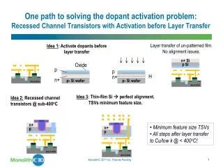
One path to solving the dopant activation problem:Recessed Channel Transistors with Activation before Layer Transfer Layer transfer of un-patterned film. No alignment issues. Idea 1: Activate dopants before layer transfer n+ Si Oxide p Si p p H p- Si wafer n+ p- Si wafer n+ Idea 3: Thin-film Si perfect alignment. TSVs minimum feature size. Idea 2: Recessed channel transistors @ sub-400oC n+ • Minimum feature size TSVs • All steps after layer transfer to Cu/low k @ < 400oC! n+ p p MonolithIC 3D Inc. Patents Pending