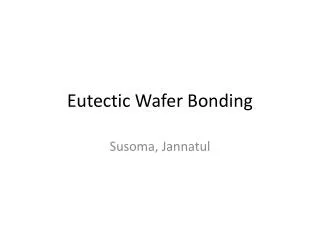
Wafer Bonding
Wafer Bonding. By:- Nishant Malik. Contents. Introduction to wafer bonding Classification Fusion Bonding Anodic Bonding Thermocompression Bonding Eutectic Bonding Glass Frit Bonding Adhesive Bonding Comparison. Introduction .


Wafer Bonding
E N D
Presentation Transcript
Wafer Bonding By:- Nishant Malik
Contents • Introduction to wafer bonding • Classification • Fusion Bonding • Anodic Bonding • Thermocompression Bonding • Eutectic Bonding • Glass Frit Bonding • Adhesive Bonding • Comparison
Introduction • Wafer bonding is a process that temporarily or permanently joins two wafers or substrates using a suitable process. • Microtechnology involves various types of bonding processes • Wafer bonding • Wire bonding • Flip chip bonding Used in IC packaging and printed circuit board assembly. Will not be covered in this lecture.
Why Wafer Bonding ? • To make Silicon on Insulator (SOI) wafers. • To create complex 3D structures and cavities which create device functionality (µ-channel). • Packaging method to create closed environments (vacuum packages for resonators, and for optical and IR devices). • Integration technology for joining 2 chips fabricated separately (CMOS + MEMS).
Fusion/Direct Bonding • Identical materials with ultra smooth (<10Å roughness) are bonded without intermediale layer. • Method • Surface preparation: O2 plasma, HF dip, hydration. • Wafers brought into contact to form weak bonds (van der wall forces, hydrogen bonding). • Annealing at 600-1200 oC to convert physical forces to chemical bonds. • Mechanism • Hydrophilic => Si – O – Si • Hydrophobic => Si – Si
Fusion Bonding: Chemistry • Hydrophilic bonding (b) Hydrophobic bonding
Fusion Bonding: Bonding Tool • Vacuum level ~ 10-5 mbar • Temperature ~ 500oC • Force ~ 1000N
Fusion Bonding: Advantages/ Disadvantages • Advantages: • No problem of thermal expansion mismatch at the interface. • The bond strength is a function of annealing temperature and can be as high as single crystal silicon. • For certain applications such as micro-turbine application, fusion bonding can be used at much higher operating temperatures. • Disadvantages: • Stringent surface roughness requirements to the order of a fraction of a nm, also surfaces must be ultra-clean. • Annealing of fusion bonded wafers above 450ºC cannot be performed if the substrate contains CMOS devices.
Anodic Bonding • Anodic bonding is also referred to as Electrostatic Bonding or Field-Assisted Thermal Bonding. This bonding process is assisted by electric field. In this method we bond a conductive silicon substrate to a glass substrate which is rich in sodium. • In 1969, Wallis and Pomerantz invented the concept of glass-metal seal bonding using assisted electric field. • Technique • Voltage applied ~ 600-1000 V • Elevated temperature ~ 200-500°C • Positive ions in glass migrate, creating depletion layer near Si surface; voltage drop creates large E-field pulling surfaces into contact.
Anodic Bonding • Silicon and glass wafers are aligned and maintained in intimate contact. • Silicon substrate is the anode and the glass metallization is the cathode. • The resultant applied electric field drive Na ions from the glass silicon interface. • The disassociated oxygen ions react with the silicon to form an irreversible silicon– oxide bond. • The primary variables in this process are time, temperature, and voltage.
Anodic Bonding: Advantages/ Disadvantages • Advantages: • Bonding is achieved at lower temperatures, 200–450 °C, which in turn gives more design flexibility. • It facilitates hermetic sealing in vacuum. • Very high strength permanent bond can be achieved with relative ease. • Parasitic capacitances are small since glass has low permeability and is usually quite thick. • Disadvantages: • Bow or warp in the wafer, which may be associated with the considerable volumetric changes undergone by the glass during anodic bonding and thermal mismatch of the substrates. • Anodic bonding generates outgassing of oxygen in particular.
Thermocompression Bonding • Thermocompression bonding is a technique for wafer packaging, using metals such as Au, Cu and Al as the bonding layer between two silicon wafers. • Method: • Metal deposited on substrates. • Bring them into intimate contact. • Apply temperature and pressure. • Diffusion of metal atoms between the surfaces, due to atomic contact between both substrates.
Thermocompression Bonding • Aluminum (Al) • bonding temperature 400 to 500 °C. • Applied force above 70 MPa • Gold (Au) • Bonding temperature 260 and 450 °C • Applied force ~ 20 MPa • Copper (Cu) • Bonding temperature 380 to 450 °C • Applied force above 15-30MPa.
Thermocompression Bonding • SiO2 can be used a diffusion barrier layer. • Annealing can be done to increase the bond strength after bonding for short duration. • Native oxide from the Cu and Al surface can be removed by forming gas treatment. • Surface roughness of wafers can be reduced by chemical mechanical planarization (CMP).
Advantages/ Disadvantages • Advantages: • Good level of hermeticity can be achieved. • Metal good conductor of heat. • Allows electrical contact and mechanical support in one step. • Easy and clean process. • Disadvantages: • High pressure requirements. • Flat surface requirements.
Eutectic bonding • Eutectic bonding is a wafer bonding technique with an intermediate metal layer that can produce a eutectic system. • Those eutectic metals are alloys that transform directly from solid to liquid state, or vice versa from liquid to solid state, at a specific composition and temperature without passing a two-phase equilibrium, i.e. liquid and solid state. • Liquid and two solid phases co-exist in equilibrium at the eutectic composition CE and the eutectic temperature TE . • The fact that the eutectic temperature can be much lower than the melting temperature of the elements is of importance. • Method: • Substrate processing • Conditioning prior to bonding (e.g. oxide removal) • Bonding process (Temperature, Mechanical Pressure for a few minutes) • Cooling process
Eutectic bonding • Eutectic reaction – transition from liquid to mixture of two solid phases, α + β at eutectic concentration CE. • At most two phases can be in equilibrium. Three phases (L,α, β) may be in equilibrium only at a few points along the eutectic isotherm. Single phase regions are separated by 2-phase regions.
Eutectic bonding: Advantages/ Disadvantages • Advantages: • good reliability • large fabrication yield • low demands on surface topography and roughness • simple process technology • high bonding strength • relatively small seal ring geometries • small device feature size possible • Disadvantages: • different CTE of intermediate layer and wafer material • restrictions of widespread connections caused by mechanical stress
Glass frit bonding • Glass frit bonding, also referred to as glass soldering or seal glass bonding, describes a wafer bonding technique with an intermediate glass layer. • Glass frit bonding can be used for many surface materials, e.g., silicon with hydrophobic and hydrophilic surface, silicon dioxide, silicon nitride, aluminum, titanium or glass, as long as the CTE are in the same range. • The glass between the wafers to be bonded is heated, so that its viscosity continually decreases until the so called wetting temperature is reached. • The glass comes into contact with the surface to be bonded at the atomic level, and flows into surface roughness and around surface steps. • Method: • Deposition of glass paste • Thermal conditioning • Bonding process • Cooling down
Glass frit bonding • The glass frit is a paste consisting glass powder, organic binder, inorganic fillers and solvents. The physics of glass frit bonding is related to the glass chemistry . When the glass wets the surface to be bonded at high temperature, thin layers of the material to be bonded are fused into the glass, so that finally after cooling, a continuous material interaction occurs which forms a strong bond. Optimal process temperature & pressure(insufficient spreading/overflow).
Glass frit bonding: Advantages/ Disadvantages • Advantages: • simple process technology • connection of different materials (different melting temperatures) • connection of rough surfaces • absence of voltage during bonding • hermetic sealing • high bonding yield • Disadvantages: • risk of mechanical stress caused by CTE mismatch • risk of glass material flowing into structures
Adhesive bonding • Adhesive bonding (also referred to as gluing or glue bonding) describes a wafer bonding technique with applying an intermediate layer to connect substrates of different materials. • The commercially available adhesive can be organic or inorganic and is deposited on one or both substrate surfaces. • Adhesives especially the wide established SU-8 and Benzocyclobuten (BCB) are specialized for MEMS or electronic component production. • Method: • Cleaning and pre-treatment of substrates surfaces • Application of adhesive, solvent or other intermediate layers • Contacting substrates • Hardening intermediate layer
Adhesive bonding • Hardening of the adhesives are possible: • at room temperature • through heating cycles • using UV light • by applying pressure Adhesion layer Softbake
Adhesive bonding • Adsorption theory, based on wetting of a surface. • Like most bonding techniques, based on the fact that atoms and molecules adhere to each other when they are brought in sufficiently close contact. • For wetting to occur, the solid surface must have a greater surface energy than the liquid.
Adhesive bonding: Advantages/ Disadvantages • Advantages: • wide range of adhesives adjusted for MEMS and electronic components • feasibility at vacuum or different atmospheric gases • simple and low cost process • low bonding temperature ≤ 200 °C • absence of electric voltage and current • applicable to various wafer materials • compensation of surface non-uniformities and contamination • high transparency • Disadvantages: • penetration of moisture • no hermetic seals with organic materials • limited long-term stability in harsh environments • limited temperature stability • relatively low bond strengths
Reference • Andreas PloÈûl*, Gertrud KraÈuter, Wafer direct bonding: tailoring adhesion between brittle materials, Materials Science and Engineering, R25 (1999) 1-88 . • Shawn J. Cunningham and Mario Kupnik, Chapter 11Wafer Bonding, MEMS Materials and Processes Handbook. • G. Wallis, D.I. Pomerantz: Field-assisted glass-metal sealing, J. Appl. Phys. 40, 3946–3949 (1969). • Ji Fan and Chuan Seng Tan, Chapter 4 Low temperature wafer-level metal thermocompression bonding technology for 3D integration, Metallurgy-Advances in Materials and Processes. • Sumant Sood, Shari Farrens, Ron Pinker, James Xie and Wilbur Cataby, Al-Ge Eutectic Wafer Bonding and Bond Characterization for CMOS Compatible Wafer Packaging, ECS Transactions, 33 (4) 93-101 (2010). • Peter Ramm, James Jian-Qiang Lu, Maaike M.V. Taklo, Handbook of Wafer Bonding. • F. Niklaus, G. Stemme, J. -Q. Lu, and R. J. Gutmann, Adhesive wafer bonding, J. Appl. Phys., 99, 2006. • Roy Knechtel, Glass frit bonding: an universal technology for wafer level encapsulation • and packaging, Microsyst Technol (2005) 12: 63–68.