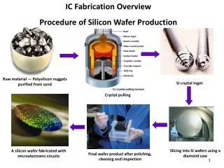
Wafer Fabrication
Wafer Fabrication. CZ processing. k o = C s /C o increases as ingot grows The dopant concentration is given by: I L =I o (1+V s /V o ) ko and C s = -dI L /dV s = C o k o (1-f) ( k o-1). Ingot diameter varies inversely with pull rate:. L = latent heat of fusion N = density


Wafer Fabrication
E N D
Presentation Transcript
CZ processing ko = Cs/Co increases as ingot grows The dopant concentration is given by: IL=Io(1+Vs/Vo)ko and Cs = -dIL/dVs = Coko(1-f)(ko-1) Ingot diameter varies inversely with pull rate: L = latent heat of fusion N = density s = Stephan-Boltzman constant km = thermal conductivity at Tm Tm = melt temperature (1417 oC for Si) C, I and V are concentration, number of impurities and volume when o: initial L: liquid and s: solid
Float Zone Processing Liquid Temperature Solid Cs Co CL Concentration In Float Zone refining, solid concentration varies with initial concentration as follows:
Typical defects in crystals Typical defects are: Point defects – vacancies & interstitials Line defects – dislocations Volume defects – stacking faults, precipitates The equilibrium number of vacancies varies with temperature: nv = noexp(-Ev/kT) O and C are also defects with concentrations of 1017-1018 cm-3 and 1015-1016 cm-3 Other impurities are in the ppb range Thermal stresses cause dislocations. Thermal stress is: s = EaDT s = stress, E = Young’s modulus, a = thermal expansion coefficient (mm/m/oC)
Photolithography MSE 630 Fall, 2008
The way patterns are defined on thin films is called Lithography. If light is used to transfer patterns from a mask on to a wafer, then this special kind of lithography is called photolithography.
Resist Process Steps: • Spin Process Parameters: • Viscosity • Spin Speed • Step Coverage • Adhesion – surface chemistry
Factors Affecting Resist • Materials: • Glass Transition Temperature, Tg Pattern Stability • Molecular Weight Resolution • Substrate atomic number Z Proximity effects • Chemical composition Etch resistance, adhesion • Process: • Development (strength, time temperature) • Baking time • Post-treatment: scum removal, stripping native oxide
Methods of Pattern Definition • Radiation Sources: • Photons • Electrons • X-ray • Ions • Approaches: • Shadow mask • Direct write
Mask Controlled Optical Lithography
Limitations in Optical Lithography: The Diffraction Limit K1 ~ 0.6-0.8 and K2 ~ 0.5. NA is the numerical aperture number, NA=n*sin(a) where n=1 and a is the angle formed by the point light source and the aperture width Resolution: K1l/NA Depth of Focus: K2l/NA2 from microns to 50 nm
Example Estimate the resolution and depth of focus of an excimer laser stepper using KrF light source (l = 248 nm) and NA=0.6 Assume k1 = 0.75 and k2 = 0.5. Solution: R = k1*l/NA = 0.75(0.248/0.6) = 0.31 nm DOF = ± k2*l/NA2 = ±0.5(0.248/(0.6)2) = ±0.34 mm
Shrinking device size drives need for finer replication methods:
Electron Beam Direct Write Performance Details down to 20 nm Alignment within 50 nm
Limitations to e-Beam Lithography • Resolution factors: • Affected by beam quality – ability to focus on surface (~1 nm) • Blurred by secondary electrons (lateral range – a few nm • Resolution factors: • Affected by beam quality – ability to focus on surface (~1 nm) • Blurred by secondary electrons (lateral range – a few nm • Performance: • On organic resist PMMA ~7 nm • Inorganic resist ~ 1-2 nm
Limitations Increasing the electron beam energy (keV) or decreasing the resist layer results in broadening at the surface
Wet Chemical Treatment • Substrate Cleaning • Fuming HNO3 • H2SO4/H2O2 • HCL/H2O2 • NH4OH/H2O2 • Resist Technology • Keytone Solvents • Acetone • Isopropanol (IPA) • Mask Removal • Fuming HNO3 • Wet Etching • Strong Acids/Bases Many steps are involved and repeated in producing an integrated circuit including: resist application and removal, substrate cleaning, and etching
Etching Challenges Actual etch profiles that can occur. (a) Lateral etching under mask (b) rounded photoresist which is further eroded during etching, leading to even more lateral etching. (b) also illustrates etch selectivity
Dry Etching Characteristics High Resolution Profile control
Reactive Ion Etch (RIE) A diagram of a common RIE setup. An RIE consists of two electrodes (1 and 4) that create an electric field (3) meant to accelerate ions (2) toward the surface of the samples (5). Ion species react with substrate, and remove material by sputtering and chemical reaction
Thin Film Deposition Methods Evaporation: electron gun resistance heating electrically biased flux Sputtering: Ion beam Plasma Chemical Vapor Deposition (CVD)
Chemical Vapor Deposition (CVD) Steps involved in the CVD process. Gas species (1) is attracted to the surface (2), where it reacts to form surface compounds (3,4) and gases (5) which rejoin the gas stream (6,7) CVD systems (a) atmospheric cold-wall system for deposition of epitaxial silicon, (b) low-pressure hot-wall system for deposition of polycrystalline silicon and amorphous films, e.g. polysilicon and silicon dioxide, respectively.
Typical thin-film problems Step coverage of metal over nonplanar topography. (a) shows conformal step coveage, with constant thickness on horizontal and vertical surfaces, (b) shows poor step coverage. Thin film filling issues. (a) good metal filling of a via or contact hole in a dielectric layer. (b) shows silicon dioxide dielectric filling the space between metal lines, with poor filling leading to void formation, and (c) shows poor filling of the bottom of a via hole with a barrier or contact metal.
Sputtering Important processes in sputter deposition
Physical Vapor Deposition (PVD) Schematic diagrams of PVD systems and processes
Electroplating Sub-micron features with high aspect rations are easily achieved via electroplating
Thin Film Deposition Issues • Surface Coverage • Surface diffusion • Flux directionality • Film Morphology • Temperature • Ion Treatment • Stress • Thermal • Growth Induced • Adhesion • Compatibility to film substrate • Stress • Beneficial role of few nm of Ti, Cr, or NiCr
Step Coverage Directional evaporation leaves sides of structures uncovered Temperature and gas pressure change the mean free path of the atoms, thus influencing coverage profiles
Diffusion is not constant across cross section, and continues with every subsequent high-temperature step; hence, we use charts as below to calculate surface concentrations, Cs, from average conductivity,
Effective diffusion-time, (Dt)eff, is the sum of the diffusivity and time at each step: (Dt)eff= D1t1+D1t2(D2/D1)=D1t1+D2t2 Effective diffusivity is: DAeff=Do+D-(n/ni)+D=)n/ni)2 for N-type DeffA=Do+D+(p/ni)+D++(p/ni)2 for P-type Values are tabulated, as in table 7.5