Download
1 / 16
420 likes | 1.78k Vues
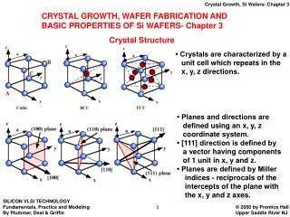
CRYSTAL GROWTH, WAFER FABRICATION AND BASIC PROPERTIES OF Si WAFERS- Chapter 3. Crystal Structure. • Crystals are characterized by a unit cell which repeats in the x, y, z directions. . • Planes and directions are defined using an x, y, z coordinate system.

E N D
CRYSTAL GROWTH, WAFER FABRICATION AND BASIC PROPERTIES OF Si WAFERS- Chapter 3 Crystal Structure • Crystals are characterized by a unit cell which repeats in the x, y, z directions. • Planes and directions are defined using an x, y, z coordinate system. • [111] direction is defined by a vector having components of 1 unit in x, y and z. • Planes are defined by Miller indices - reciprocals of the intercepts of the plane with the x, y and z axes.
• Silicon has the basic diamond crystal structure - two merged FCC cells offset by a/4 in x, y and z. See 3D models http://jas.eng.buffalo.edu /education/solid/unitCell/home.html • Various types of defects can exist in crystal (or can be created by processing steps. In general these are detrimental to device performance.
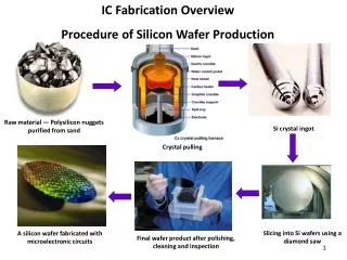
Crystal Growth • Si used for crystal growth is purified from SiO2 (sand) through refining, fractional distillation and CVD. • The raw material contains < 1 ppb impurities. Pulled crystals contain O (≈ 1018 cm-3) and C (≈ 1016 cm-3), plus any added dopants placed in the melt. • Essentially all Si wafers used for ICs today come from Czochralski grown crystals. • Polysilicon material is melted, held at close to 1417 ˚C, and a single crystal seed is used to start the growth. • Pull rate, melt temperature and rotation rate are all important control parameters.
(More information on crystal growth at http://www.memc.com/co-as-description-crystal-growth.asp Also, see animations of http://www.memc.com/co-as-process-animation.asp) (Photo courtesy of Ruth Carranza.))
• An alternative process is the float zone process which can be used for refining or single crystal growth. • After crystal pulling, the boule is shaped and cut into wafers which are then polished on one side. (See animations of crystal polishing etc. at http://www.memc.com/co-as-process-animation.asp)
Modeling Crystal Growth • We wish to find a relationship between pull rate and crystal diameter. • Freezing occurs between isotherms X1 and X2. • Heat balance: latent heat of crystallization + heat conducted from melt to crystal = heat conducted away. (1)
• The rate of growth of the crystal is (2) where vP is the pull rate and N is the density. (3) • Neglecting the middle term in Eqn. (1) we have: • In order to replace dT/dx2, we need to consider the heat transfer processes. • Heat radiation from the crystal (C) is given by the Stefan-Boltzmann law (4) • Heat conduction up the crystal is given by (5)
• Differentiating (5), we have (6) (7) • Substituting (6) into (4), we have • kS varies roughly as 1/T, so if kM is the thermal conductivity at the melting point, (8) (9) • Solving this differential equation, evaluating it at x = 0 and substituting the result into (3), we obtain (see text): (10) • This gives a max pull rate of ≈ 24 cm hr-1 for a 6” crystal (see text). Actual values are ≈ 2X less than this.
Modeling Dopant Behavior During Crystal Growth • Dopants are added to the melt to provide a controlled N or P doping level in the wafers. • However, the dopant incorporation process is complicated by dopant segregation. (11) • Most k0 values are <1 which means the impurity prefers to stay in the liquid. • Thus as the crystal is pulled, NS will increase.
• If during growth, an additional volume dV freezes, the impurities incorporated into dV are given by (12) (13) (14) • We are really interested in the impurity level in the crystal (CS), so that (15) (16) where f is the fraction of the melt frozen.
• Plot of Eq. (16). • Note the relatively flat profile produced by boron with a kS close to 1. • Dopants with kS << 1 produce much more variation in doping concentration along the crystal. • In the float zone process, dopants and other impurities tend to stay in the liquid and therefore refining can be accomplished, especially with multiple passes • See the text for models of this process.
Modeling Point Defects in Silicon • Point defects (V and I) will turn out to play fundamental roles in many process technologies. • The total free energy of the crystal is minimized when finite concentrations of these defects exist. (17) • In general and both are strong functions of temperature. • Kinetics may determine the concentration in a wafer rather than thermodynamics. • In equilibrium, values for these concentrations are given by: (18) (19)
• V and I also exist in charged states with discrete energies in the Si bandgap. • In N type Si, V= and V- will dominate; in P type, V+ and V++ will dominate. • Shockley and Last (1957) first described these charged defect concentrations (see text). Note: • The defect concentrations are always << ni. ( doping EF point defect concentrations) • As doping changes, the neutral point defect concentrations are constant. • However, the charged defect concentrations change with doping. \ the total point defect concentrations change with doping. (20) (21)
Example (see text for details): • At 1000 ˚C, the P region will be intrinsic, the N region is extrinsic. Note: • ni relative to doping in the two regions. • V0 is the same in the two regions. • Different charge states dominate in the different regions.
Oxygen and Carbon in CZ Silicon • The CZ growth process inherently introduces O and C. • Typically, CO ≈ 1018 cm-3 and CC ≈ 1016 cm-3. • The O in CZ silicon often forms small SiO2 precipitates in the Si crystal under normal processing conditions. • O and these precipitates can • actually be very useful. • • Provide mechanical strength. • • Internal gettering (described • later in Chapter 4).
Summary of Key Ideas • Raw materials (SiO2) are refined to produce electronic grade silicon with a purity unmatched by any other commonly available material on earth. • CZ crystal growth produces structurally perfect Si single crystals which can then be cut into wafers and polished as the starting material for IC manufacturing. • Starting wafers contain only dopants, O, and C in measurable quantities. • Dopant incorporation during crystal growth is straightforward except for segregation effects which cause spatial variations in the dopant concentrations. • Point, line, and volume (1D, 2D, and 3D) defects can be present in crystals, particularly after high temperature processing. • Point defects are "fundamental" and their concentration depends on temperature (exponentially), on doping level and on other processes like ion implantation which can create non-equilibrium transient concentrations of these defects. • For more information see papers @ http://www.memc.com/t-technical-papers.asp