Download
1 / 1
20 likes | 269 Vues
Mechanical Arm. Pressing Chamber. Mold containing template and thin film. Hydraulic Jack. Indium-Thallium (In-21at%Tl) Nanowires.

E N D
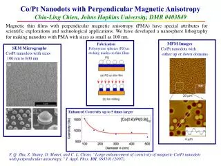
Mechanical Arm Pressing Chamber Mold containing template and thin film Hydraulic Jack Indium-Thallium (In-21at%Tl) Nanowires Various diameters of In-21at%Tl nanowires fabricated (750nm, 380nm, 280nm, 70nm, 33nm). For nanowires of diameters >70nm, twins observed at room temperature along entire length of nanowires 1 2 3 Future Work • Fabricate In-21at%Tl nanowires of smaller diameter • Fabricate NiMnCoIn nanowires from produced thin films Hierarchical Manufacturing and Modeling for Phase Transforming Active Nanostructures D.C. Lagoudas a, K. Gall b, I. Karaman c, X. Zhang c, J. Kameoka d a Department of Aerospace Engineering, Texas A&M University, College Station, Texas 77843-3141; b School of Materials Science and Engineering, Georgia Institute of Technology, Atlanta, GA 30332-0250; c Department of Mechanical Engineering, Texas A&M University, College Station, Texas 77843-3123; d Department of Electrical and Computer Engineering, Texas A&M University, College Station, Texas 77843-3128 Fabrication and Properties of MSMA Thin Films Project Objectives Multiscale Modeling Framework and Simulation Educational Goals Overall Concept Fabrication of Monolithic and Hybrid SMA and MSMA Nanowire Fabrication of Nanofiber Membrane for Protein Detection Sputtering System Nanowire Fabrication Procedure Electrospinning of Silica Nanofiber Membrane • Solution: a mixture of spin on glass coating (SOG), polyvinylpyrrolidone (PVP), and butanol. • Solution concentration: PVP 0.04 g/ml, SOG:butanol = 4:1 in volume ratio. • Processing parameters: feeding rate: 8 ul/min, applied voltage: 7 kV, deposition distance: 5 cm, heating temperature: 500°C for 12h. • PVP was removed during the heating. Resultant silica membrane was composed of nanofiber with ~100 nm in diameter. Magnetron sputtering system for multilayer film depositions. The system has four magnetron guns capable of DC and RF sputtering and is able to obtain a base pressure of 10-8 Torr or better. A load lock is attached to the system to increase the throughput of the system. Anodized Aluminum Oxide (AAO) Template (Empty) NiMnGa Thin Films Performance of Protein Detection NiMnGa Thin Films weredeposited on several substrates. Mn-rich target with the composition of Ni49.5Mn30Ga20.5 was used. The composition was tailored by varying the deposition power. • Understand the effect of nanoscale manufacturing on reversible martensitic phase transformations • Develop low-cost and easily scalable nanomanufacturing techniques that will allow fabrication of shape memory alloy (SMA) and magnetic shape memory (MSMA) alloy nanowires • Fabricate higher scale structures and devices from nanowires and hybrid thin films • Use multiscale modeling framework to guide the fabrication process, reveal fundamental multi-scale physical phenomena in reversible phase transformation, and aide design of higher scale devices • Fabrication of nanofiber membrane for protein detection • Random-distributed electrospun nanofibers formed a porous membrane. The membrane is incorporated in the layered structure of the detector. • The sensitivity is improved due to the small diameter of nanofibers and the resultant extremely large surface area to volume ratio. Filled AAO template after extrusion In-21at%Tl Nanowires in Cross-Section of AAO The as-deposited films were partly crystalline as seen in the xrd pattern The DSC plot shows reversible martensite to austenite phase transformation TEM Dark field image of 70nm diameter nanowire showing BCT twins at room temperature TEM dark field image of 200nm diameter nanowire showing BCT twins at room temperature SEM image of silica spun nanofibers Schematic of nanofiber membrane protein detector • Modeling In-21at%Tl bulk • and nanowires • Developing new potentials based on ab initio calculations RT Above Af • The detection limit is 32 times lower than traditional 96-well enzyme-linked immunosorbent assay (ELISA). • The detection time is 1h compared to ELISA’s 1 day Nanoscale Martensitic Transformation Mechanisms in NiTi TEM Dark field image of 33nm diameter nanowire at room temperature TEM Dark field image of 70nm diameter nanowire with constant crystal structure at 100°C Multilayer twinned B19’ Below Mf As-deposited film shows grains with needle shaped texture indicating martensite, distributed in a seemingly amorphous matrix. Above Af, the diffraction pattern shows a significant change in SADP along with grain growth. Change in SADP was again observed when cooled below Mf Selected Area Electron Diffraction (SAED) patterns of 33nm diameter nanowire at room temperature NiMnCoIn Thin Films • Surface energy will reduce as twin width increases • Agree well with the experimental observation 1 • DSC curve of an as deposited, • amorphous freestanding • Ni50Co6Mn38In6 film. The film • was heated/cooled/heated at a • rate of 80 °C/min. 2 • For 70nm diameter nanowires, reversible phase transformation observed from BCT martensite to FCC austenite • For 33nm diameter nanowires, SAED patterns indicate FCC crystal structure (austenite) at room temperature 3 • Graduate a diverse group of students prepared for research on • nanotechnology with an interdisciplinary and global outlook • Motivate undergraduates, particularly those from • underrepresented groups, to continue to graduate school and • research careers • Educate undergraduate and K-12 students and teachers on • technology, its benefits, and to communicate the excitement of • discovery of science Compared with shuffling to B19 two layers of atoms out of four layers one layer of atoms out of two layers shuffling • DSC curves of crystallization • process in freestanding • Ni50Co6Mn38In6 films heated linearly • at different rates. The effective • crystallization energy was • calculated to be 86.59 kJ mol-1.