Download
1 / 13
130 likes | 427 Vues
Temperature Dependent Electrical Properties in Oxide Thin Films. Timothy Nagle Gerald R. Taylor Jr. Physics Department James Madison University AAPT - Chesapeake Section Loyola College Baltimore, MD April 21, 2001. Outline. Introduction Why study ITO films? Techniques

E N D
Temperature Dependent Electrical Properties in Oxide Thin Films Timothy Nagle Gerald R. Taylor Jr. Physics Department James Madison University AAPT - Chesapeake Section Loyola College Baltimore, MD April 21, 2001
Outline • Introduction • Why study ITO films? • Techniques • Methods and Apparatus • Results • Electrical properties and microstructure • Conclusions • Future work
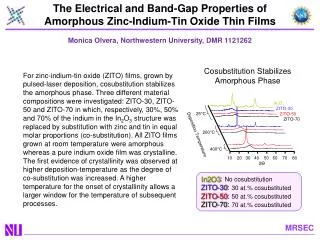
Indium Tin Oxide (ITO) • Deposited by rf magnetron sputtering • 2738-3811 Å thickness • Hall effect measurements • 77K, 273K, 298K • r, Ne, m, RH • How does T effect r? • 77K - 298K • What is the microstructure?
Hall Effect • Current (I) normal to magnetic field (B) • Force (F) acts on charge carrier • F normal to I and B • Hall Voltage (VHall) between A and A’
Hall Effect Data • Carrier concentration • Ne = 2 × 1021 cm-3 • Little variation with T (77K<T<298K) • Mobility • m = 24 cm2/V×s • Hall Coefficient • RH = 2.5 × 10⁻³ cm3/C • negative charge carriers
Optical Characterization • Absorption at 400 nm • Photons absorbed into e • e = h×c/l = 3.10 eV
ITO Microstructure • ~6000 Å thick • Feature height • 10-30 nm • Grain size • 130 nm • Mean Free Path • l=t×vth • l= 10 nm
Conclusions • Temperature range 77K - 298K • little variation in Ne, m, RH • ITO behaves like impurity metal or degenerate semiconductor • r increases linearly with T • phonon scattering • 130 nm grain size • l = 10 nm << grain size
Acknowledgements • Dr. David Lawrence • Geoff Stenger • Dr. Chris Hughes • Dr. Brian Augustine • Brian Woodley