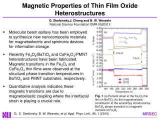
Thin Gate Oxide Growth & Reliability: MOSFET's Technological Evolution
Explore the evolution of Thin Gate Oxide growth in MOSFET technology, from 1980 to 2003, the key breakthroughs, reliability requirements, oxide scaling, and innovations enabling the scaling from 90nm to 22nm. Understand gate dielectric scaling, oxide charges, traps, requirements, growth techniques, characteristics, and technologies involved in thin oxide growth processes, such as thermal oxidation and rapid thermal annealing. Learn about typical thin gate oxide processes in vertical furnaces, including growth rates, cleaning procedures, vertical and horizontal furnace comparisons, and gate oxide characterizations for strength and reliability assessments.

Thin Gate Oxide Growth & Reliability: MOSFET's Technological Evolution
E N D
Presentation Transcript
THIN GATE OXIDE Growth and Reliability
The main character of our story: The MOSFET • No other human artifact has been fabricated in larger numbers (except perhaps nails?) • “…some consider it one of the most important technological breakthroughs in human history…”(Wikipedia, the source of all human knowledge)
1980 → 1985 → 1988 → 1991 → 1994 → 1999 → 2003 … LGATE = 10 μm 5 μm 2.5μm 1.3 μm 0.63 μm 0.25 μm 130 nm …. 1980 → 1985 → 1988 → 1991 → 1994 → 1999 → 2003 … LGATE = 10 μm 5 μm 2.5μm 1.3 μm 0.63 μm 0.25 μm 130 nm …. 1980 → 1985 → 1988 → 1991 → 1994 → 1999 → 2003 … LGATE = 10 μm 5 μm 2.5μm 1.3 μm 0.63 μm 0.25 μm 130 nm …. 1980 → 1985 → 1988 → 1991 → 1994 → 1999 → 2003 … LGATE = 10 μm 5 μm 2.5 μm 1.3 μm 0.63 μm 0.25 μm 130 nm …. 1980 → 1985 → 1988 → 1991 → 1994 → 1999 → 2003 … LGATE = 10 μm 5 μm 2.5μm 1.3 μm 0.63 μm 0.25 μm 130 nm …. 1980 → 1985 → 1988 → 1991 → 1994 → 1999 → 2003 … LGATE = 10 μm 5 μm 2.5μm 1.3 μm 0.63 μm 0.25 μm 130 nm …. 1980→ 1985 → 1988→ 1991 → 1994 → 1999 → 2003 … LGATE = 10 μm 5 μm 2.5 μm 1.3 μm 0.63 μm 0.25 μm 130 nm …. Scaling • Shrink dimensions maintaining aspect-ratio • Must shrink electrostatic features as well (depletion regions→ doping level and profiles) ↔ 1 μm
LECTURE OBJECTIVES • Understand the importance and requirement of thin gate oxide • Able to describe the technique to grow high quality thin oxides • Understand the nature of Mode-A,B &C of breakdown failure • Able to calculate the oxide strength, τBDand QBD
Scaling from 90 nm to 22 nm and innovations that enable the scaling
Gate Oxide L GATE Gate Oxide n+ n+ ID P-well
Gate Oxide Requirements • Possible to grow thin oxide precisely and uniformly across the wafer • Adequate reliability characteristics under operating conditions in terms of strength (Breakdown Voltage), Reliability of operation over specified time (τBD, QBD) and resistance to hot-carrier degradation)
Desired Gate Oxide Characteristics • The thickness closely match the specification in MOSFET design • Uniform across the wafer, from wafer to wafer, run to run. • Small interface charge • High dielectric strength • Long lifetime under normal operating conditions • High resistance to hot-carrier damage
Technology of Thin Oxide Growth • Oxidation furnace Vertical furnace is more favorable compared to horizontal. 3 reasons: • Wafer/wafer holders make no contact with oxidation tube during loading, growth and unloading (fewer particles generated). • Lighter boat material can be used, as a result, better heat and gas distributions (result in better oxide uniformity). • Precise control of wafer to wafer spacing.
Technology of Thin Oxide Growth 2. Control of Growth Rates • Slow growth rates required to reproducibly grow thin oxides with precise thickness. • Grow in dry O2 at atmospheric pressure at lower temperatures (800-900C). • Growth at reduced total pressure, or reduced O2 partial pressure
Technology of Thin Oxide Growth Typical Thin Gate Oxide Process • Carried out in vertical furnace • Prior to oxide growth; • Grow and strip sacrificial oxide (to remove defect in silicon layer) • Cleaning procedure (normally generic of RCA cleaning) • Loaded by robotic wafer handling at specific insertion rates ~ 15 cm per minute for 150mm wafer, 10cm per minute for 200mm wafer. Furnace temperature ~ 650 – 700C.
Technology of Thin Oxide Growth Typical Thin Gate Oxide Process • Furnace temperature is ramped up to the growth temperature. During temperature ramp up, N2 or Ar is purged to prevent unwanted growth. • Temperature stabilisation around 5 min before O2 is released. • Dry oxidation at atmospheric pressure at temperature ~ 800-900C. Some companies use dry/wet/dry to control the thermal budget. Others use HCl, TCA , DCE as chlorine source.
Technology of Thin Oxide Growth Typical Thin Gate Oxide Process • Wafers subjected to Post Oxidation Annealing (POA) in N2 at ~100C. The purpose is to minimise the interface trap density by neutralising the dangling bond of Si with H atoms. This will improve the τBD and QBD. • Furnace temperature is ramped down, and wafer is unloaded at certain rate.
Gate Oxide Characterisations • Gate oxide Strength • Breakdown voltage, then calculate the breakdown electric field. • Gate Oxide Reliability a) τBD – time to breakdown b) QBD – charge to breakdown
Gate Oxide Strength Definition – The maximum electric field strength that can be applied to the oxide before it breaks down. Unit MV/cm. Test procedure – Ramped Voltage Test using MOS capacitor
Gate Oxide Strength T1 GATE Gate Oxide T2 substrate • A voltage that is increase linearly with time (ramp voltage, ∆V / ∆t) is applied between the gate and substrate of MOS test structure until oxide breakdown. • Breakdown is defined at the voltage value VBD at which a sudden voltage drop across the oxide is observed. • Ramp voltage between T1 and T2, measure current. • The sudden voltage drops at the electrode is detected using a sensing resistor.
Gate Oxide Strength Ig V V VBD t • Take the voltage at the voltage drop as the breakdown voltage (VBD) • Calculate the oxide strength by VBD / oxide thickness
Example Thin oxide of 50nm is stressed under voltage ramp test until it breaks at 1 V. Calculate the oxide strength. Oxide strength = Breakdown voltage / oxide thickness = 1 V / 5e-6 cm = 0.2e6 V/cm = 0.2 MV / cm
Mode of Breakdown Failure A histogram is usually used to plot the results of the ramped-voltage tests (oxide strength) of a group of oxide samples (normally up to 1000 capacitor tested to characterized certain oxidation process recipe), with the no of group that failed within each voltage interval (within each 1 MV/cm) Breakdown Frequency Mode-B (2-6 MV/cm) Mode-C (8-12 MV/cm) Mode-A (<1 MV/cm) 5 10 Breakdown Field, MV/cm
Mode-A • Fail instantly upon the application of a small gate bias. • Its believed that this oxide may experienced a gross defect such as pinholes and may already be shorted before the application of low strength field.
Mode-B • Fail at electric field of intermediate strength (2-6 MV/cm) • Contain weak spots that do not produce instant shorting, but may give rise to early failures of ICs under normal operating conditions. • Majority of oxide breakdown failure in sub-micron CMOS fall under this category. Mostly due to the defects exist in the oxide.
Mode-B • Defects include; • Sodium contamination – originated from W furnace filament, chemicals • Metal contamination – from substrate, other processes • Surface roughness at Si-SiO2 interface from etching or cleaning procedures – promote localize weak spot • Non-uniformity of oxide growth • Crystalline defect – defect originated during crystal growth
Mode-C • Can withstand the highest electric fields (8-12 MV/cm) • Failure mechanism always referred as intrinsic failure. • Generally assumed as defect-free oxide. • Several models proposed to explain the intrinsic breakdown
Mode-C • Models to explain the intrinsic breakdown • Holes generation and trapping model. Electrons are injected into the conduction band of oxide by FN tunneling. In the oxide, these electrons are accelerated towards the gate, and generate electron-hole pair in the oxide. These generated holes are trapped at the localised areas and in return trap positive oxide charge. This will increase the positive charge at certain point in the oxide, causing the tunneling current density to increase there up to critical point where the breakdown occurs. • Wolters Electron Lattice-Damage Model
Gate Oxide Reliability Gate oxide strength is not directly relevant to the normal device operation, since what is really needed is how long the thin oxide will survive at lower field strength. The measurement of oxide performance at lower electric field is called Time-Dependent Dielectric Breakdown (TDDB). • 1) Time to Breakdown under Constant-Voltage Stressing (τBD) • 2) Time to Breakdown under Constant-Current Stressing (τBD) • Charge to Breakdown (QBD)
Gate Oxide Reliability Time to Breakdown under Constant-Voltage Stressing Electric field in the oxide is held constant (voltage is held constant) during the stress test. The length of time, τBD elapsed until breakdown occurs is then measured.
Gate Oxide Reliability Time to Breakdown under Constant-Current Stressing. - An alternative to constant-voltage test. Current is injected into the oxide by Fowler- Nordheim tunneling, and this value Jinj is held constant. Voltage and time are recorded until breakdown occurs.
Charge to Breakdown In a constant-current test; - QBD is charge-to-breakdown. - The product of current density and tBD QBD = Jinj . τBD In a constant voltage test;
Gate Oxide Reliability Emperical Model to Estimate Oxide Reliability Applicable to Mode-B and Mode-C Failures 1. QBD for intrinsic oxide is approximately constant for small FN tunneling current. 2. Qp (hole charge to breakdown) also constant. Qp = Jpα τBD sec , G=350 MV/cm Where at 300 °C
Example Calculate the time-to-breakdown, τBD at 300K of 8nm defect free gate oxide, use inCMOS technology with Vcc 5.0V. τBD (300K)= 1e-11 (sec) exp (350e6 . Tox / Vox) = 1e-11 exp (350e6 . 8e-7 / 5.0) = 2e13 sec
HOMEWORK Calculate the minimum thickness of a defect free oxide that could be used in a MOSFET that is to operate at 5.5V for 10 years at 150 C (423K) without suffering oxide breakdown. Given G(423K)= 283 MV/cm and Τ0 (423K)=0.75e-11 sec. Comment on reliability of the MOSFET to actually survive 10 years without breakdown. tox min = 87.82 Å <- This is the answer