Download
1 / 27
270 likes | 440 Vues
Room-temperature fabrication of high-k gate oxide with sol-gel process. Experiment. Surface sol-gel gate dielectric with sol-gel active layer. High leakage current to be suppressed, b ut device characteristics can be observed. Experiment. Source-drain electrode pattern.

E N D
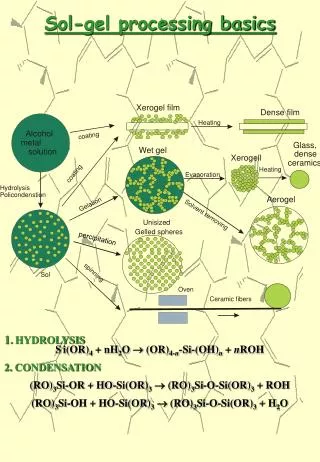
Room-temperature fabrication of high-k gate oxide with sol-gel process
Experiment • Surface sol-gel gate dielectric with sol-gel active layer High leakage current to be suppressed, but device characteristics can be observed
Experiment • Source-drain electrode pattern (Many reference, especially paper about gate dielectrics) (In our experiment) Gate leakage current is proportional to electrode overlap area Drain current is proportional to channel W/D ratio
Experiment • SSG active layer Poor device characteristic, but showed potential
Experiment Next step: low temperature ZnO aqueous ink (2008) 150ºC “Sol-gel on chip” process (2011) 230ºC Enables polyimide substrate (Endure 275ºC)
Thermal annealing Generally sol-gel process requires thermal annealing Elimination of residual impurities Densification of porous as-deposited film Establishing Zr-O bondings Zr-O bondings became more ionic
Thermal annealing In case of surface sol-gel process (~50% carbon content of spin-coating sol-gel) Desorption spectra: Large amount of C and H are eliminated by thermal annealing XPS composition analysis (as-deposited film) ZrO2 – Zr : C : O = 1.0 : 3.7 : 4.0 Al2O3 – Al : C : O = 1.0 : 2.0 : 1.9 Many carbon impurities inside as-deposited sol-gel film
Thermal annealing Table – composition after 500ºC thermal annealing (Carbon ~5%) Dielectric breakdown is related to- Local alignment of traps (voids, carbon impurities, and so forth)
Plasma treatment Plasma treatment Improved insulating property of HfO2 dielectric film
Plasma treatment • Plasma treatment • Removal of residual alkoxides and hydroxyl groups • Hf 4f7/2 and Hf 4f5/2energy levels: • Binding energies of the Hf–O bonds • Increased binding energy: • Advancement of the O-Hf-O bonds • Plasma treatment completes oxidation
Plasma vs. UV Comparison between UV treatment and Plasma treatment Plasma treatment Low leakage current when combined with thermal annealing UV treatment Low leakage current with room-temperature UV irradiation Photolysis Densification
UV treatment Mechanism of photolysis of precursor titanium(IV) di-n-butoxidebis(2-ethylhexanoate) Sol-gel precursor is used like photopolymer (365nm UV irradiation)
UV treatment Mechanism of photolysis of precursor Carbon-based peaks on FTIR spectra is decreased by UV irradiation After 20mins of exposure : Organic groups in the film mostly disappeared 2870~2957cm-1 1200~1800cm-1
UV treatment Mechanism of photolysis of precursor XPS reveals UV irradiation effectively removed carbon-based residuals (Comparable to 400ºC annealing) Annealing at 400ºC UV irradiation As-deposition
UV treatment Mechanism of photolysis of precursor Film was processed in RT condition but, Sol-gel film was fully oxidized from interface to surface (Green line: carbon) Carbon concentration was slightly higher than 400ºC film
UV treatment Mechanism of photolysis of precursor With UV irradiation, volatile products are collected and investigated by MS analysis → Products are carbon oxide and hydrocarbons Carbon monoxide Carbon dioxide Butane Heptanal Heptene Heaptane
UV treatment Proposed photolysis mechanism: To explain reaction product, reactions shown on schematic were proposed 2→3: By ligand-to-metal charge transfer (LMCT) transition, excited molecule is thermally unstable and may dissociate 3→5: Titanium in an oxidation state of three is typically unstable, resulting decomposition 5→TiO2: Titanium in an oxidation state of two is very reactive and obtain oxygens from the ligands Simple explanation: Titanium is oxidized by accepting electrons
UV treatment Room-temperature fabrication of ZrO2 gate dielectric General precursor: Zinc acetylacetonate in DMF, with MEA Sol-gel film is irradiated with ultraviolet (UVA,UVB,UVV)
UV treatment Proposed photolysis mechanism: By 15min UV irradiation Carbon residuals are almost removed Zr:O composition ratio = 1:2 (Only indicated in XPS) Yet did not produce a functional ZrOx film with high dielectric constant Photolysis is done, but densification is not yet → Longer treatment is required for high-k
UV treatment Thickness: 6.3 nm ZrOx, 4.3 nm interface layer Capacitance: Increased with UV irradiation Leakage current: Decreased with ODPA passivation Capacitance : Insulation – Trade-off relation
UV treatment Comparison with surface sol-gel dielectric Surface sol-gel Capacitance: 757nF/cm2 Gate leakage: ~10-5A/cm2 (without passivation) 500ºC-processed UV-cured sol-gel Capacitance: 320nF/cm2 Gate leakage: ~10-7A/cm2 (with ODPA passivation) RT-processed
UV treatment Comparison with surface sol-gel dielectric Dielectric constant is lower than SSG film Lower density of spin-coating ZrO2 film Thicker/or lower capacitance of interface layer
UV treatment Comparison with surface sol-gel dielectric Both sol-gel processed ZrO2 film have relatively high gate leakage current Passivation is required for suppress gate leakage
Passivation layer Passivation layer degrade gate capacitance Thickness of passivation layer has to be minimized to maximize capacitance of gate dielectric stack
Passivation layer Ultrathin coating of polyimide • Typical spin-on polymers cannot yield conformal • and pin-hole-free films in the sub-100 nm regime • With cross-linkable poly(amicacid), 9nm coating • of polyimide thin film is possible • → Still to thick • Self-assembled monolayer enables ultrathin film • → Ideal for purpose, but thermal stability?
Passivation layer Ultrathin coating of polyimide • Polyimide-like SAM is not reported yet • Polymer deposition by Langmuir-Blodgett technique • STM image of polyimide LB film
Conclusion & Future work • Conclusion • With UV irradiation treatment, device-level gate dielectric can be fabricated • To minimize gate leakage current, proper passivation layer is required • Future work • (Gate Dielectric) • S/D pattern redesign • (Active layer) • Optimum thickness experiment • (Low temperature gate dielectric) • UV irradiation treatment with SSG/Spin-coated dielectric film • Device fabrication with “sol-gel on chip” semiconductor layer • → All-soluble, low-temperature processed thin film transistor