Download
1 / 18
180 likes | 312 Vues
Improving insulating property of sol-gel processed gate dielectrics. Surface sol-gel ZrO 2 dielectric. Ta doping on ZrO 2 gate dielectric 10 2 times lower leakage current. As applied electric field is increased, Effectiveness of Ta-doping in decreased. Surface sol-gel ZrO 2 dielectric.

E N D
Improving insulating property of sol-gel processed gate dielectrics
Surface sol-gel ZrO2 dielectric Ta doping on ZrO2 gate dielectric 102 times lower leakage current As applied electric field is increased, Effectiveness of Ta-doping in decreased
Surface sol-gel ZrO2 dielectric Rough surface increases leakage current Surface sol-gel film has relatively larger RMS (compared with ALD film)
High-k/polymer bilayer dielectric Successful TFT fabrication with SSG dielectric Using bilayer dielectric (HfO2/Polystyrene) → 103 times lower leakage current by improved rms
High-k/polymer bilayer dielectric Decreased capacitance value 21.1nm PS has very low capacitance (k = 2.6)
High-k/polymer bilayer dielectric Bilayer organic/inorganic gate dielectric Thinner polymer layer – less capacitance degradation Using UV epoxy layer as polymer dielectric (Thickness is decreased during cross-linking)
High-k/polymer bilayer dielectric Bilayer organic/inorganic gate dielectric Low RMS value: 0.3nm ALD HfO2 film is very smooth RMS is slightly increased after organic coating
High-k/polymer bilayer dielectric • Bilayer organic/inorganic gate dielectric • As polymer layer is thin (10nm), capacitance degradation is minimized. • Insulating property is also good (Ig < 10-7) • Limitations: • Low-k value of polymer layer • Cannot endure active layer sol-gel coating process (high temp. annealing)
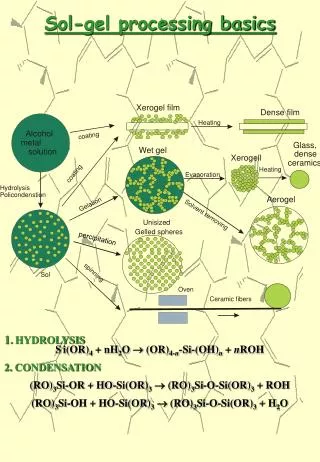
Inorganic smoothing layer Thin, smooth coating of inorganic thin film General sol-gel spin-coating Gelation in acid-catalyzed condition Decreasing precursor conc. Decreasing hydrolysis rate Decreasing acidity
Inorganic smoothing layer Thin, smooth coating of inorganic thin film 1.8nm ultrathin film from 3g ZrCl4/l RMS – 0.3nm after 500ºC annealing Si Wafer 1.8nm ZrO2
Inorganic smoothing layer Chemical solution deposition of ZrO2 Zr(C3H7O)4 : hydrolysis in water Hydroxide precipitation in citric acid and H2O2 Hydroxide re-dissolved by NH4OH addition Thin film <5nm easily achieved by spin-coating (very fine particle in colloid solution) Citric acid:Zr
Inorganic smoothing layer Chemical solution deposition of ZrO2 Smooth film – RMS < 0.5nm Not very dependent to precursor concentration and citric acid concentration
Inorganic smoothing layer 10nm Chemical solution deposition of ZrO2 Smooth film – RMS < 0.5nm Thicker film tends to crystallize Ultrathin film maintained low RMS after annealing 20nm 40nm 3nm
Inorganic smoothing layer Chemical solution deposition of ZrO2 High k~20, not dependent to citric acid concentration Relatively higher leakage current (compared with SSG dielectric)
Gate leakage suppression Plasma treatment Improved insulating property of HfO2 dielectric film
Gate leakage suppression • Plasma treatment • HfCl4 precursor and 250ºC annealing • Removal of residual alkoxides and hydroxyl groups • Hf 4f7/2 and Hf 4f5/2energy levels: • Binding energies of the Hf–O bonds • Increased binding energy: • Advancement of the O-Hf-O bonds • Plasma treatment completes oxidation
Gate leakage suppression Plasma treatment Treatment was more effective than HfO2 case Plasma → annealing was effective But annealing → plasma was not
Conclusion & Future work • Conclusion • Bilayer dielectric is effective for reducing gate leakage current density • Plasma treatment is effective for reducing gate leakage current density • Future work • (Gate Dielectric) • Increasing thickness of SSG dielectric : 20 cycles → 30,40 cycles • Adopt sol-gel smoothing layer • Oxygen plasma treatment • (Active layer) • SnO2 active layer (New precursor: Tin tert-butoxide) • Ta-doped SnO2 active layer • (Sol-gel on chip) • Equipment setup • (Revised paper) • Transmittance/Sheet resistance data of WAW electrode, Band diagram, Ti electrode