Download

1 / 12
120 likes | 186 Vues
Gate Oxide Integrity And Microloading Characterization of 300mm Process Tools. Abstract author: K. Mautz Motorola, Semiconductor Products Sector. Wei Yan 09-26-02. Introduction . Characterizations on gate oxide integrity from 300mm diffusion furnaces

E N D
Gate Oxide Integrity And Microloading Characterization of 300mm Process Tools Abstract author: K. Mautz Motorola, Semiconductor Products Sector Wei Yan 09-26-02
Introduction • Characterizations on gate oxide integrity from 300mm diffusion furnaces • Microloading effects on 300mm Etch and CMP tools • Experimental data and results are from SEMICONDUCTOR300-- a JV between Motorola and Infineon Technologies
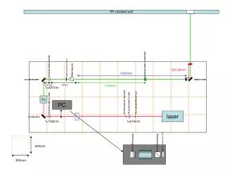
Experimental • For GOI study • The 300mm test wafers consisted of a 45nm SiN ARC layer on 800nm of BPSG annealed over silicon, and imaged with a DRAM or logic pattern. • For microloading study • The CMP 300mm test wafer consisted of 800mm BPSG-annealed oxide film overlying a patterned 165mm TEOS oxide film, covered with a 5.5 nm liner nitride film to serve as a delineation layer during cross-sectional analysis, or overlying a 200nm Cap nitride layer patterned with the logic pattern.
GOI measurement • Mercury probing is the technique used to measure the amount of charge contained in the oxide. • The GOI measured values were considered to be within an acceptable range between the 300mm and 200mm wafer furnaces. • The main difference was a large and increasing hysteresis behavior on successive wafer runs.
Incoming particle contamination levels • Contamination on the wafer can cause unintentional changes in electrical properties of the devices. • To prevent contamination, up to 25% of all wafer manufacture processing consists of cleaning steps. • The amount of electrically active impurities in oxides must be minimized because embedded impurities attract of repel free charges in the underlying silicon. • Device performance depends strongly on the concentration of free charges in the silicon
Procedures a silicon oxide layer heavily doped with boron and phosphorus, (Boron-Doped Phosphosilicate Glass-BPSG). FOR MORE INFO... CMP polishing Planarization
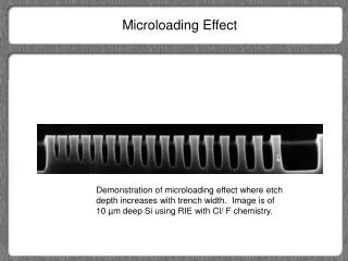
Microloading effects on Etch process • Microloading causes non-uniformity on etch process and affects the etch depth on Etch process • Etch rate uniformity variation from the wafer’s center to edge tend to magnify the microloading effects • Contact/via features tend to be most susceptible to these effects. • Standard Etch process resulted in significant microloading effects between the contact holes and interconnect features. It can be reduced by adjusting the etch process parameter
Chemical Mechanical Polishing • CMP is heavily used in the IC manufacturing. • CMP has the ability to planarize over longer length scales tha traditional planarization techniques • The CMP process is carried out by pressing a rotating wafer face down into a moving polishing pad covered with a suitable slurry.
Competitive Analysis, cont. • Typical CMP Setup http://pubweb.northwestern.edu/~xji626/ FOR MORE INFO...
Microloading effects on CMP • Some observable oxide dishing or significant erosion of the nitride lines was observed on the isolated linewidth features where the polish stopped on the nitride film. • Plug recess is where the damascene structure sits slightly lower than the field area due to the faster removal rate than the field. • Dishingoccurs when the polishing pad under the pressure of polishing, is able to deform into the damascene structure and polish it below the field area • Erosion of the field material occur due to the enhanced polishing at the edges of the structures, the corners of the field area are exposed and erode more rapidly than unpatterned areas.
Microloading effects on CMP • When polishing a wafer that has step features, only the top of the features tough the polishing pad, concentrating the pressure on these contact points. This increase the polishing rate above that of a blanket wafer. • It causes nonuniformity in the removal rate across patterns of different densities due to variations in the pressure distribution across the pattern.
Conclusion • The GOI measured values were considered to be within an acceptable range. • The etch process characterization showed significant microloading effects between the contact holes and interconnect features. • The CMP analysis indicated that there was only a small difference in planarity and microloading between the 300mm and 200mm wafer comparable tools and processes