Download
1 / 19
240 likes | 624 Vues
Original Authors: S. K. Han, G. P. Heuss, H. Zhong, v. Misra, and C.M. Osburn Class Presentation by: Joseph Wu. Etching of High K Gate Dielectric and Gate Metal Electrode Candidates. Outline. Background/ terminology Experiment setup Etching recipe for metal gate electrode

E N D
Original Authors: S. K. Han, G. P. Heuss, H. Zhong, v. Misra, and C.M. Osburn Class Presentation by: Joseph Wu Etching of High K Gate Dielectric and Gate Metal Electrode Candidates
Outline • Background/ terminology • Experiment setup • Etching recipe for metal gate electrode • Pt and TaN wet etching • RuO2 and Ru etching • Etching recipe for High K gate dielectrics • Conclusion
Background • CMOS trend : smaller chips and more functionalities => shorter channel length and thinner gate oxide => problems encountered • Problems with ultra-thin polysilicon and SiO2 – polysilicon depletion – Current leakage through gate oxide – Degradation and breakdown of gate oxide – Dopant penetration through gate oxide • Possible solution : metal gate and high k dielectrics
The MOS Transistor • MOSFET : Metal-Oxide-Semiconductor Field Effect Transistor which is used for switch and amplification in electronics. • NMOS : a MOSFET with n-type source and drain • PMOS : a MOSFET with p-type source and drain Ref: http://web.cs.mun.ca/~paul/transistors/node1.html
Terminology • PVD - Physical vapor deposition • MBE - Molecular bean epitaxy • RTCVD - Rapid thermal CVD • RPECVD – Remote plasma enhenced CVD • MOCVD – Metalorganic CVD • BOE – Buffer oxide etchants • Hf – Hafnium • Zr – Zirconium • La – Lanthanum • Y - Yttrium • Ta - Tantalum
Experimental • Two different RIEs • 100TP (324 cm2) from SEMI GROUP • SLR720 (248 cm2) from PLASMA THERM • Parallel electrodes • 13.56 Hz radio frequency power
MBE RHEED: reflection high energy electron diffraction Kingetsu, Toshiki Surface and technology of Advance Materials 2 (2001) 331-347
PVD • The process involves striking a high current, low voltage electric arc directly on the target material to produce an instantaneous ionization of the metal. • These metal ions are propelled at high energies into the vacuum through either an inert or reactive gas and is subsequently deposited onto the substrate of interest. • E.g. sputtering
PVD - Sputtering Ref: http://personal.cityu.edu.hk/~appkchu/AP4120/7.PDF
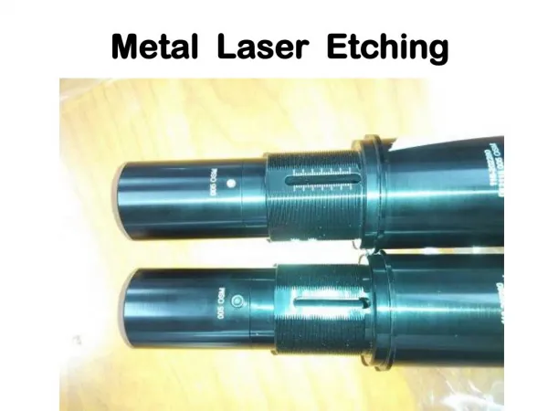
Pt and TaN Wet Etching • Limited photoresist stability and adhesion to the substrate => rebake the photoresist at 115 oC for every 5 minutes for Pt and 10 minutes for TaN • Pt oxide layer inhibit etching => Ar+ ion milling performed at 80 Watts, 20 sccm at 60 mtorr for 3 minutes • Nitrogen content in TaN influences resistivity and etching rate => require further research
RuO2 and Ru Etching • Use RIE and O2 plasma • O2 plasma has poor selectivity to the photoresist => add 2.5% CHF3 • Achieve Ru etching rate to 5nm/min => add a few percent of Cl2
MOCVD Machida H. et. al. Journal of Crystal Growth 237-239 (2002) 586-590
RTCVD http://personal.cityu.edu.hk/~appkchu/AP4120/7.PDF
JVD Ref: T.P. Ma. Applied Surface Science 117/118 (1997) 259-267
Etching of High-K Dielectrics • Factors influence etching characteristics • Material • Deposition system • Substrate pretreatment • Post deposition anneal conditions
Conclusion • Need for exploring new materials for the metal gate and high k dielectrics • Different reactors are shown • Etching recipe provided for advanced CMOS technology