Download
1 / 2
30 likes | 227 Vues
h . Light Emission From an Ambipolar Semiconducting Polymer Field Effect Transistor James Swensen, Cesare Soci and Alan J. Heeger UC Santa Barbara DMR- 0099843 Program Director: Dr. Andrew J. Lovinger.

E N D
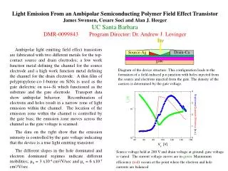
h Light Emission From an Ambipolar Semiconducting Polymer Field Effect Transistor James Swensen, Cesare Soci and Alan J. HeegerUC Santa BarbaraDMR-0099843 Program Director: Dr. Andrew J. Lovinger Ambipolar light emitting field effect transistors are fabricated with two different metals for the top-contact source and drain electrodes; a low work function metal defining the channel for the source electrode and a high work function metal defining the channel for the drain electrode. A thin film of polypropylene-co-1-butene on SiNx is used as the gate dielectric on n++-Si which functioned as the substrate and the gate electrode. Transport data show ambipolar behavior. Recombination of electrons and holes result in a narrow zone of light emission within the channel. The location of the emission zone within the channel is controlled by the gate bias; the emission zone moves across the channel as the gate voltage is scanned. The data on the right show that the emission intensity is controlled by the gate voltage indicating that the device is a true light emitting transistor. The different slopes in the hole dominated and electron dominated regimes indicate different mobilities; µh = 3 x10⁻⁴cm2/V/sec and µe = 6 x10⁻⁵ cm2/V/sec. Drain-Ca Source-Ag gate Diagram of the device structure: This configuration leads to the formation of a field-induced p-n junction with holes injected from the source and electrons injected from the gate. The density of the carriers is determined by the gate voltage. Source voltage held at 200 V and drain voltage at ground; gate voltage is varied. The current voltage curves are in green. Maxiumum efficiency (red)occurs at the point where the electron and hole currents are balanced
Light Emission From an Ambipolar Semiconducting Polymer Field Effect Transistor James Swensen, Cesare Soci and Alan J. HeegerUC Santa BarbaraDMR-0099843 Program Director: Dr. Andrew J. Lovinger Education: This is a clear example of interdisciplinary research. The successful demonstration of the light emitting Field effect transistor involves a combination of materials science, device science, semiconductor physics and the chemistry of new materials. The elimination of trapping sites at the interface with the dielectric was an essential feature required to obtain ambipolar injection and transport. Outreach: The results described briefly above were published in Applied Physics Letters 87, 253511 (2005).