Download
1 / 27
320 likes | 740 Vues
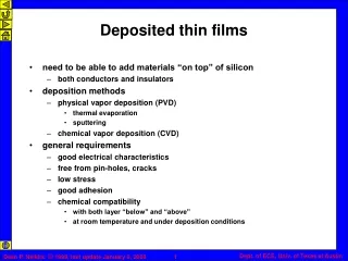
Deposited thin films. need to be able to add materials “on top” of silicon both conductors and insulators deposition methods physical vapor deposition (PVD) thermal evaporation sputtering chemical vapor deposition (CVD) general requirements good electrical characteristics

E N D
Deposited thin films • need to be able to add materials “on top” of silicon • both conductors and insulators • deposition methods • physical vapor deposition (PVD) • thermal evaporation • sputtering • chemical vapor deposition (CVD) • general requirements • good electrical characteristics • free from pin-holes, cracks • low stress • good adhesion • chemical compatibility • with both layer “below” and “above” • at room temperature and under deposition conditions
Kinetic theory of gases • for a gas at STP: • N ~ 2.7 x 10¹⁹ molecules/cm3 • N µ pressure • one atmosphere = 1.0132 x 10⁵ pascal = 1.01 bar = 760 Torr (mm Hg) • 1 Pascal = 1/132 Torr ~ 10-5 atms • fraction of molecules traveling distance d without colliding is • l is the mean free path • at room templ ~ 0.7 cm / P (in pascals) ~ 5.3 x 10⁻³ cm / P (in Torr) • at room temp and one atmosphere l ~ 0.07 µm
Velocity distribution • for ideal gas, velocity distribution is Maxwellian • we’ll use • ~ 900 miles/hour at rm temp • rate of surface bombardment (flux) • j = 3.4 x 10²² (# / cm2 • sec) • P / √MT • P in Torr, M is gram-molecular mass • monolayer formation time t • # molecules per unit area / bombard rate
Impact of pressure on deposition conditions • pressure influences • mean free path: l µ1/P • “contamination rate” : t µ1/P rough vacuum high vacuum very high vacuum
270˚ incidence randomizing collisions 180˚ randomizing collisions source 180˚ incidence Impact of pressure on deposition conditions • material arrival angular distribution • depends on mean free path compared to both size of system and size of wafer “steps” • Case I: “atmospheric pressure”: 760 Torr Æl = 0.07 µm • l << system & steps • isotropic arrival on ALL surfaces • flat surfaces: 180˚ • inside corners: 90˚ Æ thinner • outside corners: 270˚ Æ thicker substrate assume material does NOT migrate after arrival!!
180˚ incidence source substrate 180˚ incidence assumes material does NOT migrate after arrival!! randomizing collisions “low” pressure: l << system,l > step • Case II: 10-1 Torr Æl = 0.5 mm • small compared to system, large compared to wafer features • isotropic arrival at “flat” surface • BUT no scattering inside “hole”!! • top flat surface: 180˚ • “inside” surface: depends on location! • shadowing by corners of features • “anisotropic” deposition no randomizing collisions
no randomizing collisions source substrate assumes material does NOT migrate after arrival!! “vacuum” conditions: l > system, l >> step • case III: 10-5 Torr Æl = 5 meters • long compared to almost everything • anisotropic arrival at all surfaces! • geometric “shadowing” dominates • anisotropic deposition • “line-of-sight” deposition • very thin on “side walls” • very dependent on source configuration relative to sample surface
Physical vapor deposition: thermal evaporation • high vacuum to avoid contamination • “line-of-sight” deposition, poor step coverage • heating of source material • potential problem: thermal decomposition • rates ~ 0.1- few nm/sec • typically Pvapor ~ 10-4 Torr immediately above source • “pressure” at sample surface is much lower • few monolayers per sec Æ Pequiv ~ 10-6 Torr
Thermal evaporation • main heating mechanisms • resistively heat “boat” containing material • tungsten (mp 3410˚C), tantalum (mp 2996˚C), molybdenum (mp 2617˚C) very common “heater” materials • reaction with boat potential problem • electron beam evaporator electron beam • source material “directly” heated by electron bombardment • can generate x-rays, can damage substrate/devices • Ibeam ~ 100 mA, Vacc ~ kV Æ P ~ kWatts • inductively heat material (direct for metals) • essentially eddy current losses
Sputtering • use moderate energy ion bombardment to eject atoms from target • “purely” physical process • can deposit almost anything from the SIMS WWW server http://www.simsworkshop.org/WWW/Siteinfo/gifstoshare/SIMSlogo1.gif adapted from: Campbell, p. 295
plasma E field B field plasma E field B field target target planar magnetron S-gun conical magnetron adapted from: Campbell, p. 298 Sputtering • plasma generates high density, energetic incident particles • magnetic field used to confine plasma, electric field (“bias”) to accelerate • dc plasma: metals • rates up to ~1 µm / minute • rf plasma: dielectrics • typically inert (noble) gas used to form incident ions • ion energies ~ few hundred eV ; ejected atoms ~ tens eV • ~10-2 Torr, l ~ 5 mm • better step coverage than evaporation
Chemical vapor deposition • general characteristic of gas phase chemical reactions • pressures typically atmospheric to 50 mTorr • l ranges from << 1 µm to ~ 1 mm • reactions driven by • thermal: temperatures 100˚ - 1000˚ C • higher temperature processes increase surface migration/mobility • plasma • optical • example materials • polycrystalline silicon (poly) • silicon dioxide • phosphosilicate, borosilicate, borophosphosilicate glasses • PSG, BSG, BPSG • silicon nitride
CVD system design: hot wall reactors • heat entire system: thermally driven reactions • requires leak-tight, sealed system • avoid unwanted contamination, escape of hazardous materials (the reactants) • atmospheric: high deposition rates • low pressure (LPCVD): lower rates, good uniformity plasma assisted CVD: PECVD
Cold wall reactors • heat substrate “only” using • resistive heating (pass current through “susceptor”) • inductive heating (external rf fields create eddy currents in conductive susceptor) • optical heating(lamps generate IR, absorbed by susceptor) • advantages • reduces contamination from hot furnace walls • reduces deposition on chamber walls • disadvantages • more complex to achieve temperature uniformity • hard to measure temperature • inherently a non-isothermal system
gas flow lines x d substrate gas flow lines substrate Gas flow in CVD systems • purely “turbulent” flow • reactants are well mixed, no “geometric” limitations on supply of reactants to wafer surface • typical of LPCVD tube furnace design • interaction of gas flow with surfaces • away from surfaces, flow is primarily laminar • friction forces velocity to zero at surfaces • causes formation of stagnant boundary layer • v: velocity; r: density; µ: viscosity • reactant supply limited by diffusion across boundary layer • geometry of wafers relative to gas flow critical for film thickness uniformity • to improve boundary layer uniformity can tilt wafer wrt gas flow
Basic configurations • parallel plate plasma reactor • horizontal tube reactor • “pancake” configuration is similar • barrel reactor • single wafer systems from: http://www.appliedmaterials.com/products/pdd.html
Material examples: polysilicon • uses • gates, high value resistors, “local” interconnects • deposition • silane pyrolysis: 600˚-700˚ C SiH4Ž Si + 2H2 • atmospheric, cold wall, 5% silane in hydrogen, ~1/2 µm/min • LPCVD (~1 Torr), hot wall, 20-100% silane, ~hundreds nm/min • grain size dependent on growth temperature, subsequent processing • 950˚ C phosphorus diffusion, 20 min: ~1 µm grain size • 1050˚ C oxidation: ~1-3 µm grain size • in-situ doping • p-type: diborane B2H6: r ~ 0.005 W-cm (B/Si ~ 2.5x10⁻³) • can cause substantial increase in deposition rate • n-type: arsine AsH3, phosphine PH3 : r ~ 0.02 W-cm • can cause substantial decrease in deposition rate • dope after deposition (implant, diffusion)
Metal CVD • tungsten • WF6 + 3H2D W + 6HF • cold wall systems • ~300˚C • can be selective • adherence to SiO2 problematic • TiN often used to improve adhesion • causes long “initiation” time before W deposition begins • frequently used to fill deep (“high aspect ratio”) contact vias • aluminum • tri-isobutyl-aluminum (TIBA) • LPCVD • ~200˚-300˚ C, tens nm/min deposition rate • copper • Cu b-diketones, ~100˚-200˚ C
CVD silicon dioxide • thermally driven reaction • mid-temperature: ~ 500˚C • “LTO” (low-temp. oxide) T < ~500˚C • SiH4 + O2Ž SiO2 + H2 • cold-wall, atmospheric, ~0.1 µm/min • hot-wall, LPCVD, ~0.01 µm/min • plasma-enhanced reaction (PECVD) • low temperature: ~250˚C • high temperature: ~700˚C • tetraethyl orthosilicate (TEOS) • Si(OC2H5)4Ž SiO2 + by-products • new materials • low “k” dielectrics • interlevel insulation with lower dielectric constants (k < ~3) • fluorinated oxides, spin-on glasses, organics • high k dielectrics: k > ~25-100’s • gate insulators, de-coupling caps
Phosphosilicate glass (PSG) • good barrier to sodium migration • can be used to “planarize” topography using “glass reflow” • plastic flow of PSG at T > ~1000˚C • deposition • add phosphine during pyrolysis of silane4PH3 + 5O2Ž 2P2O5 + 6H2 • P2O5 incorporated in SiO2 • problems / limitations • for reflow, need high P content to get appreciable flow at “reasonable” time/temps • P2O5 is VERY hygroscopic • for > ~ 8% P2O5 can cause corrosion of Al • normally limit to < ~ 6%
0% P 2.2% P reflow: 1100˚C, steam, 20 min q 4.6% P 7.2% P adapted from: Sze. 2nd ed., p. 256. Glass reflow process • to “even out” step edges can use plastic flow of overcoating dielectric • usually last “high” temperature step • “first fusion” • wet, high T ambient • densifies, prepares layer for window etch • only small reflow if T < 1000˚C • second fusion • after contact windows are etched • can be wet or dry ambient
BPSG, 850˚C / 30min BPSG, 1050˚C / 20sec BPSG 4%/4%, as deposited Rapid flow and BPSG • can add both phosphorus and boron to glass • ~4% P and ~4% B • avoids hygroscopicity problems, lowers glass transition temperature • examples • PSG, 8% P, 950˚C / 30 min: no appreciable reflow • BPSG, 4% each, 830˚C / 30min: 30˚ flow angle • can also use rapid thermal process for heating from: J. S. Mercier, Rapid flow of doped glasses for VLSI fabrication, Solid State Technology, July 1987, p. 87.
Silicon nitride Si3N4 • uses • diffusivity of O2, H2O is very low in nitride • mask against oxidation • protect against water/corrosion • diffusivity of Na also very low • protect against mobile ion contamination • deposition • stoichiometric formulation is Si3N4 • in practice Si/N ratio varies from 0.7 (N rich) to 1.1 (Si rich) • LPCVD: ~700˚C - 900˚C • 3SiH4 + 4NH3Ž Si3N4 + 12H2 ; can also use Si2Cl2H2 as source gas • Si/N ratio 0.75, 4-8% H • r ~ 3 g/cm3 ; n ~ 2.0; k ~ 6-7 • stress: ~10 Gdyne/cm2, tensile • PECVD: ~250˚C - 350˚C • aSiH4 + bNH3Ž SixNyHz + cH2 • aSiH4 + bN2Ž SixNyHz + cH2 • Si/N ratio 0.8-1.2, ~20% H • r ~ 2.4-2.8 g/cm3 ; n ~ 1.8-2.5; k ~ 6-9 • stress: ~2C - 5T Gdyne/cm2
Safety issues in CVD • most gases used are toxic, pyrophoric, flammable, explosive, or some combination of these • silane, SiH4 • toxic, burns on contact with air • phosphine • very toxic, flammable • ammonia • toxic, corrosive • how to deal with this? • monitor! • limit maximum flow rate from gas sources • helps with dispersal problem associated with gases • double walled tubing, all welded distribution networks
Epitaxy • growth of thin crystalline layers upon a crystalline substrate • heteroepitaxy • dissimilar film and substrate • autoepitaxy • same film and substrate composition • techniques • Vapor-Phase Epitaxy (VPE) • CVD: Metal-organic VPE (MOCVD, OMVPE, ...) • PVD: Molecular Beam Epitaxy (MBE) • Liquid-Phase Epitaxy (LPE) • mainly for compound semiconductors • Solid-Phase Epitaxy • recystallization of amorphized or polycrystalline layers • applications • bipolar, BiCMOS IC's • 2-5 µm in high speed digital • 10-20 µm in linear circuits • special devices • SOI, SOS • HEMT, MODFET, HBT
Summary Slide • Deposited thin films • Kinetic theory of gases • Physical vapor deposition: thermal evaporation • Sputtering • Chemical vapor deposition • next topic: epitaxy