Thin films technologies for SRF EUcard2 WP12.2 Thin films prospectives
340 likes | 723 Vues
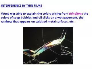
Thin films technologies for SRF EUcard2 WP12.2 Thin films prospectives. C. Z. ANTOINE, CEA, Irfu, SACM, Centre d'Etudes de Saclay, 91191 Gif-sur-Yvette Cedex, France. Outlook. Introduction Characterization tools Deposition technique Physics of SRF and advanced superconductors

Thin films technologies for SRF EUcard2 WP12.2 Thin films prospectives
E N D
Presentation Transcript
Thin films technologies for SRFEUcard2 WP12.2 Thin films prospectives C. Z. ANTOINE, CEA, Irfu, SACM, Centre d'Etudes de Saclay, 91191 Gif-sur-Yvette Cedex, France
Outlook • Introduction • Characterization tools • Deposition technique • Physics of SRF and advanced superconductors • Multilayers • Conclusion
Introduction Claire Antoine Eucard2 WP12 Meeting @ Saclay
Why thin films ? 2 reasons Making cheaper cavities : Bulk like Nb on copper (1-5 µm) Overcoming Nb monopoly: Nb3Sn, MgB2, Multilayers… • Advantages • Can also be deposited onto copper • Higher Tc => higher Q0 • Higher HSH or HC1 => higher accelerating field • Disadvantages • Fabrication and surface preparation (at least) as difficult as for bulk • Superconductivity very sensitive to crystalline quality (lower in thin films for now) • Deposition of innovative (compound) materials is very difficult • Theoretical limit (HSHvs HC1) still controverted => choice of ideal material !? • Nb : l~50 nm => only a few 100s nm of SC necessary • (the remaining thickness= mechanical support only) => Make thin films ! • Advantages • Thermal stability (substrate cavity = copper) • Cost • Innovative materials • Optimization of RBCSpossible • Disadvantages • Fabrication and surface preparation (at least) as difficult as for bulk • Superconductivity very sensitive to crystalline quality (lower in thin films for now) Claire Antoine Eucard2 WP12 Meeting @ Saclay
Thin films Challenges: depends on the strategy Optimizing structure/composition of the films on samples Optimizing deposition inside cavities • Advantages • Structure /composition can be optimized with conventional techniques • Ideal structure and composition can be achieved on model sample (guide for deposition of cavities) • Cost • Disadvantages • RF performances cannot be directly measured • Specific measurement tools need to be developed (sample cavity, magnetometer…) • Ultimately a cavity deposition set-up will be needed, but with a known aimed structure • Advantages • RF testing easy and gives direct performance • Work is done only once, direct cavity production • Disadvantages • Very heavy and lengthy, many parameters • Need to develop a specific cavity deposition set-up • Difficult to optimize set-up and film together • Optimization of the structure/composition of the film is difficult Claire Antoine Eucard2 WP12 Meeting @ Saclay
Structure of the task 12.2 (EUCARD2) • Niobium on copper (µm) • After ~ 20 years stagnation : new revolutionary deposition techniques • Great expectations in cost reduction • No improved performances/ bulk Nb • Higher Tc material (µm) • Based on superheating model. • Higher field and lower Q0 expected • Higher Tc material (nm), multilayer • Based on trapped vortices model (Gurevich) • Higher field and lower Q0 expected • Recent experimental evidences • Specific characterization tools needed • Better understanding of SRF physics needed Subtask 1 Subtask 2 Subtask 3 Claire Antoine Eucard2 WP12 Meeting @ Saclay
Characterization tools developments(task 3) Claire Antoine Eucard2 WP12 Meeting @ Saclay
“Sample cavities” • Quadrupole resonnator developed at HZB • See O. Kugeler’s talk (HZB activities) • TE011 cavity developped at IPNO Claire Antoine Eucard2 WP12 Meeting @ Saclay
Differential Locking Amplifier Excitation/Detection coil (small/sample) = T/Tc Local magnetometry developed @CEA • Measurement of HC1 on sample without edge/demagnetization effect • (local measurement: field decreases quickly far from the coil: rcoil = 2,5 mm; rsample~1 cm ~ rcoil x 4 ) Bz(a,u,) 0 Br (a,u,) 0 1 2 3 4 5 6 r/r0 0 1 2 3 4 5 6 r/r0 Claire Antoine Eucard2 WP12 Meeting @ Saclay
Deposition techniques Issues(task 1 and task 2) Claire Antoine Eucard2 WP12 Meeting @ Saclay
3 majors deposition techniques • High-energy deposition techniques • line of sight techniques • issues: getting uniform thickness/structure • limited in complex geometry • Thermal diffusion films • limited compositions available • non uniform composition • Chemical techniques CVD, ALD • conformational even in complex shape • very quick for large surfaces • issues: get the proper crystalline structure Claire Antoine Eucard2 WP12 Meeting @ Saclay
Deposition techniques: International situation • CERN • Nb bulk like: Magnetron sputtering, HPIMS (collaboration with Sheafield University) • Nb3Sn (diffusion furnace) : in project • Grenoble INP • ML: ALD and CVD • STFC • Nb, ML: PVD and ECR –CVD • Jlab and collaborators • At Jlab : ECR, HPIMS • AlmedaCorpn: CED (Plasma) • W&M : magnetron sputtering + Complete material characterization • Cornell • Nb3Sn (diffusion furnace) • Temple University • MgB2 (HP-CVD), ML in collaboration with LANL and FNAL • ANL • ML: ALD • INFN Legnaro • NbN(diffusion furnace) • Large experience on sputtering, Nb3Sn… Publications on that topic at SRF 2013: 23 Claire Antoine Eucard2 WP12 Meeting @ Saclay
HPIMS @ cern: bulk-like thin films • See G. Terenziani’s talk Claire Antoine Eucard2 WP12 Meeting @ Saclay
CVD/ ALD @ Grenoble INP • Received special R&D ALD set-up • Need to develop a suitable coordination chemistry for the ALD precursors (+ plasma ALD to help) • Process scaling up to cavity deposition will be performed with specific simulation tools. • See F. Weiss’s talk Claire Antoine Eucard2 WP12 Meeting @ Saclay
Understanding the physics of SRF(task 3)Advanced superconductors(task 2) Claire Antoine Eucard2 WP12 Meeting @ Saclay
SRF limits : back to basics • Q0 (1/Thermal dissipations) • depends on surface resistance … which depends on Tc • Higher Tc => higher Q0 => lower operation cost • Ultimate limit in Eacc: when the SC becomes dissipative! • Transition : when T and/or B↑ • Vortices in RF highly dissipative => keep Meissner state • At w < 3 GHz: we are limited by BRF!!! HC1Nb = 180-190 mT Cavities : Meissner State, no vortex please !!! Claire Antoine Eucard2 WP12 Meeting @ Saclay
SRf : HC1 vs HSH Cavities : Meissner State, H~ HC1, J~JD (@ HC1), T~2-4 K ? HSH Coils : higher TC, but mixed state (low HC1) Generally low magnetic field • Reaching higher field (Eacc/BRF) • => Reach superheating field (metastable Meissner state) : Nb3Sn, MgB2… • => Artificially enhance HC1 : Multilayers Claire Antoine Eucard2 WP12 Meeting @ Saclay
Nb3Sn: recent breakthrough • At 4,2 K Q0Nb3Sn = 20 x Q0Nb !!! • At 2 KQ0Nb3Sn ~ Q0Nb • Limited in Eacc Claire Antoine Eucard2 WP12 Meeting @ Saclay
Nb3Sn: recent breakthrough Hays. "Measuring the RF critical field of Pb, Nb, NbSn". in SRF 97. 1997. Cornell, 1997 pulsed Recent results from Cornell CW HC1Nb3Sn(~27mT) • HC1 is not a fundamental limit for SRF • but • Is it a practical limitation ? • NB : HSH is more easily observed : • Close to Tc (cf Yogi) • Pulsed RF Claire Antoine Eucard2 WP12 Meeting @ Saclay
1.5 GHz Nb3Sn cavity (Wuppertal, 1985) 1.3 GHz Nb cavity (Saclay, 1999) Nb3Sn: a lot of room for improvement HP Nb3Sn 0.03T (H°C1=0.05 T) HPNb 0.12 T (H°C1=0.17 T) Nb3Sn Nb Claire Antoine Eucard2 WP12 Meeting @ Saclay
Advanced superconductors :Multilayers Claire Antoine Eucard2 WP12 Meeting @ Saclay
B(mT) Q0 Eacc(MV/m) Alternative to bulk SC: Multilayers • Multilayers: Nb/ insulator/ superconductor / insulator /superconductor… : Surface screening and low Rs • Thin SC films. d< l => artificial enhancement of HC1* • The thin layers stand high fields without vortex nucleation • Niobium surface screening: allows higher field in the cavity • => Q0multi >> Q0Nb (SC with higher Tc than Nb) In principle : Nb I-S-I-S- Happlied HNb Cavity'sinternal surface → Outsidewall * In theory 20 nm NbN : HC1 x ~200 ** Simplified model from Gurevich Claire Antoine Eucard2 WP12 Meeting @ Saclay
Field screening / thin field Infinite plane Single layer Thin film in a uniform field B B B B Simple Model (Gurevich, 2006) Modified Model (Kubo, 2013) (1 of the reasons why measurements with Squid are ambiguous) • T. Kubo @ SRF 2013 • Made the calculation for exact boundaries condition • l, x : known bulk values (not necessary exact for thin films) • Applied to NbN, Nb3Sn, MgB2 • Similar calculation also proposed by S. Posen for Nb3Sn only Claire Antoine Eucard2 WP12 Meeting @ Saclay
Optimum thickness for SL ? • T. Kubo • SL/ML structures not effective for Nb3Sn • Contrary to simple model, very thin layers are not interesting • Optimum thickness around 100 nm for NbN ? • How does that compare with exp. Measurements ? • => Series of SL with various thicknesses (50 nm to 150 nm) is needed Claire Antoine Eucard2 WP12 Meeting @ Saclay
results from other labs [Lukaszew, W&M 2012] ~30(*) or 50 nm (**)NbN * ~ 15 nm insulator (MgO) 600(*) / 250(**) nm Nb “bulk like” MgO (100) substrate ** • Compare with what is expected for bulk Nb : ~1300 Oe @ 4.5 K ! Claire Antoine Eucard2 WP12 Meeting @ Saclay
MgB2-MgO Multilayer Films MgB2 MgO MgB2 MgO MgB2 Sapphire • Alternating MgB2-insulator structures have been fabricated on sapphire substrate: • 40 nm MgO as insulating layer, sputtered. • MgB2 deposited by HPCVD ex situ. 150, 100, and 75 nm in thickness. • Tc near 40 K for 100 and 150 nm films. Lower for 75 nm film. • Multilayer films with thin MgB2 layers show higher HC1than the 300 nm film even though the total thickness are the same. [Teng, Xi – Temple University] Claire Antoine Eucard2 WP12 Meeting @ Saclay
[Tajima, SRF 2011] Claire Antoine Eucard2 WP12 Meeting @ Saclay
Magnetometry Early results CZ Antoine, JC Villegier, G Martinet, Applied Physics Letters 102 (10), 102603-102603-4 • Magnetic screening evidenced for ML4 up to 38 mT, at T~7K • Dramatic transition around 38 mT => rcoil << rsample not valid anymore ? • Magnetometer is effective up to 1500 mA (equivalent field 150 mT) Tp° 2-40 K • Use of larger samples/smaller coil is mandatory Claire Antoine Eucard2 WP12 Meeting @ Saclay
Thermal analysis 50 nm NbN ~ 15 nm insulator (MgO) Bulk LG Nb Polycrystalline Nb substrate Large grain Nb substrate • Same calibration • Rs rf-ML2<< Rs Nb • NB. Current: ½I in Nb • ½I in NbN • Strong indication that RBCS is improved with ML • Could probably be improved with the use of thicker layers (complete screening) • Rresis higher for ML than for Nb, but strongly influenced by substrate ? • Very promising preliminary results Claire Antoine Eucard2 WP12 Meeting @ Saclay
Conclusions and perspectives • Renewed activity on bulk-like Nb films (cost issues) and high HSH SC e.g. Nb3Sn or NbN (higher performances) • ML structures seem to be a promising way to go beyond Nb for accelerator cavities • Look for higher Q0, not only Eacc ! • WE ARE ON THE EVE OF A TECHNOLOGICAL REVOLUTION FOR SRF CAVITIES ! • Few labs involved • EUCARD 2 : only large scale program in Europe in this domain, big opportunity Claire Antoine Eucard2 WP12 Meeting @ Saclay
Thank you for your attention Commissariat à l’énergie atomique et aux énergies alternatives Centre de Saclay| 91191 Gif-sur-Yvette Cedex T. +33 (0)1 69 08 73 28| F. +33 (0)1 69 08 64 42 Etablissement public à caractère industriel et commercial | RCS Paris B 775 685 019 DSM IrfuSACMLIDC2 Claire Antoine Eucard2 WP12 Meeting @ Saclay
Spares Claire Antoine Eucard2 WP12 Meeting @ Saclay
Coaxial Energetic Deposition (CED) Cathodic arc plasma. • Ions Energy 60-120 eV • Arc source is scalable for large scale cavity coatings • UHV and clean walls important Coaxial Energetic Deposition (CEDTM) Nb films grown by Jlab and AASC Almeda Applied Science Corporation. Balk like RRR values Ch. Reece; JLab
H HC2 HSH HC1 T J Claire Antoine Eucard2 WP12 Meeting @ Saclay