Download
1 / 38
740 likes | 2.7k Vues
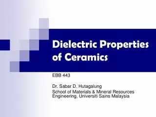
Dielectric Properties of Ceramics. EBB 443 Dr. Sabar D. Hutagalung School of Materials & Mineral Resources Engineering, Universiti Sains Malaysia. Introduction. Dielectric materials: high electrical resistivities, but an efficient supporter of electrostatic fields. Can store energy/charge.

E N D
Dielectric Properties of Ceramics EBB 443 Dr. Sabar D. Hutagalung School of Materials & Mineral Resources Engineering, Universiti Sains Malaysia
Introduction • Dielectric materials: high electrical resistivities, but an efficient supporter of electrostatic fields. • Can store energy/charge. • Able to support an electrostatic field while dissipating minimal energy in the form of heat. • The lower the dielectric loss (proportion of energy lost as heat), the more effective is a dielectric material. • Another consideration is the dielectric constant, the extent to which a substance concentrates the electrostatic lines of flux.
Dielectric Constant • The capacitance, C, of a capacitor formed by two parallel plates of area A spaced d apart with the area between the plates filled with dielectric material with a relative dielectric constant of ε is:
Dielectric Loss • For a lossy (imperfect) dielectric the dielectric constant can be represented by a complex relative dielectric constant: • The imaginary part of this complex dielectric constant, ε at a frequency, ω is equivalent to a frequency-dependent conductivity, σ(ω), given by:
Dielectric Loss • ε" is also known as the loss factor. • The small difference in phase from ideal behaviour is defined by an angle δ, defined through the equation • tan δ is known as the loss tangent or dissipation factor. • A quality factor, Q, for the dielectric is given by the reciprocal of tan δ.
Dielectric Loss Equivalent circuit diagrams: (a) capacitive cell, (b) charging and loss current, (c) loss tangent for a typical dielectric
Dielectric Loss • From Q = oAV/d = CV • If V being sinusoidal, total charge Q may be written as • Current flow on discharge of the capacitive cell in time, t: • For a real dielectric the current I has vector components IC and IR: I = IC + IR
Dielectric Loss • From magnitude of these currents, also we can define a dissipation factor, tan , as • Quality factor Q is:
Alternating Current Theory • Impedance of a resistance = R • Impedance of a capacitance = 1/iωC • Mean power, P, dissipated over a cycle in a lossy capacitor with plates of area A separated by a distance d:
Dielectric Strength • Dielectric materials are insulators (conduction cannot generally occur). • However, under certain conditions, dielectric materials can break down and conduct a significant current. • Generally, the lattice of a dielectric has sufficient strength to absorb the energy from impacting electrons that are accelerated by the applied electric field. • However, under a sufficiently large electric field, some electrons present in the dielectric will have sufficient kinetic energy to ionize the lattice atoms causing an avalanching effect. • As a result, the dielectric will begin to conduct a significant amount of current.
Dielectric Strength • This phenomenon is called dielectric breakdown and the corresponding field intensity is referred to as the dielectric breakdown strength. • Dielectric strength may be defined as the maximum potential gradient to which a material can be subjected without insulating breakdown, that is where DS is the dielectric strength in kV/mm, VB the breakdown voltage, and d the thickness.
Current-voltage characteristic up to breakdown for a typical dielectric materials
Dielectric Strength • Dielectric strength depends on • material homogeneity, • specimen geometry, • electrode shape and disposition, • stress mode (ac, dc or pulsed) and • ambient condition.
Capacitors Tantalum capacitor
Capacitors • The basic formula for the capacitance of a parallel-plate capacitor is: • To increase C, one either increases ,increases A, or decreases d. • Early capacitors consisted of metal foils separated by wax ( ~ 2.5), mica ( ~ 3 - 6), steatite ( ~ 5.5 - 7.5), or glass ( ~ 5 - 10). • The use of titania provided a significant increase ( ~ 170), was followed by perovskite-based, such as BaTiO3 ( ~ 1000).
Capacitors • DRAM chips currently utilize capacitors with Si3N4 or SiO2 as dielectric materials. • The electrodes are made of doped Si or poly-Si. • Capacitors can be fabricated onto IC chips. • They are commonly used in conjunction with transistors in DRAM. • The capacitors help maintain the contents of memory. • Because of their tiny physical size, these components have low capacitance. • They must be recharged thousands of times per second or the DRAM will lose its data.
Q = CV Q: charge (Coulomb) C: capacitance (Farad) V: potential difference (Volt) d: separation/thickness (meter) o: permitivity of vacuum = 8.854x10⁻¹² C2/m2 or F/m r: dielectric constant
Multilayer Ceramic Capacitor • The multilayer ceramic capacitor (MLCC): • where N is the number of stacked plates. • Ideally, the dielectric should have a low electrical conductivity so that the leakage current is not too large.
Multilayer Ceramic Capacitor Ceramic surface-mount capacitors. Cut-away view of multilayer ceramic capacitor.
High-K Dielectric • The bit count of MOS DRAM devices is continuously increasing. However, as bit count goes up, capacitor cell area goes down. • The capacitance per cell must remain in the 25-30 fF range, which means the capacitance density must increase. • One approach for DRAM manufacturing is to replace the traditional silicon nitride + silicon oxide with a higher dielectric constant (k) such as tantalum pentoxide (Ta2O5), Hf-oxide (HfO2) and Zr-oxide (ZrO2).
The roadmap of capacitor with DRAM technology. D.-S. Yoon et al. / Progress in Materials Science 48 (2003) 275–371
High-K Dielectric • High-k dielectric films are anticipated to be required for certain applications with low power and leakage current specifications. • High-k materials should be compatible with conventional industry standard MOSFET process flows using a poly-Si gate electrode. • HfO2, ZrO2, and Ta2O5 as high-k gate-dielectrics.
A Review of High High-k Dielectrics • Gate dielectric materials having high dielectric constant, large band gap with a favorable band alignment, low interface state density and good thermal stability are needed for future gate dielectric applications. • Ultra high-k materials such as STO (SrTiO3) or BST (BaSrTiO3) may cause fringing field induced barrier lowering effect.
A Review of High High-k Dielectrics • High-k gate dielectrics have a number of difficulties: (1) crystallization upon heating, (2) dopant penetration, (3) fixed charge, (4) low channel mobility and (5) uncontrolled oxide formation at the Si/high-k interface.
The Gate Stack Expected performance trends for complementary metal oxidesemiconductor (CMOS) transistor technologies. The unrelenting reduction in transistor size and the associated decrease in gate delay for (a) an NMOS transistor and (b) a PMOS FET are evident. Schematic illustration of important regions in a CMOS FET gate stack
EOT- equivalent oxide thickness Schematic image of MOS transistors in the year 2003 and 2013.
Physical and electrical thickness of high-k gate dielectric (ideal). SiO2 equivalent thickness EOT is smaller than high-k physical thickness.
The depletion region of thickness Wd forms adjacent to the poly-Si/oxide interface.
For example, if the capacitor dielectric is SiO2, teq = 3.90eo (A/C), eo = 8.85x10⁻³ fF/mm, thus a capacitance density of C/A=34.5 fF/mm2 corresponds to teq =10 Å. A dielectric with a relative permittivity of 16 results in a physical thickness of ~40 Å, to obtain teq =10 Å.
Comparison of (a) stacked and (b) single-layer gate dielectrics in a hypothetical transistor gate stack. Either structure results in the same overall gate stack capacitance or equivalent oxide thickness, teq =10 Å.