Download

1 / 21
210 likes | 553 Vues
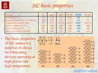
RF Dielectric Properties of SiC Ceramic Absorbers for the ARES Cavity. Yasunao TAKEUCHI. Notation. Permittivity ¢ - j r ¢ - j r . ?. Single crystal of SiC Semiconductor.

E N D
RF Dielectric Properties of SiC Ceramic Absorbers for the ARES Cavity Yasunao TAKEUCHI
Notation • Permittivity ¢ - j r ¢ - jr
? • Single crystal of SiC Semiconductor. • SiC ceramics (polycrystal structure) have larger dielectric constant and loss tangent than the single crystal SiC. • Where do these different dielectric properties come from?
!Dielectric properties are explained by the structure of the grain and grain boundary. Grain : low resistivity, p-type semiconductor Depletion layer near grain boundary : high resistivity * These dielectric properties of SiC ceramics were predicted by Dr. Maeda et al. (Hitachi co.) in 1985 .
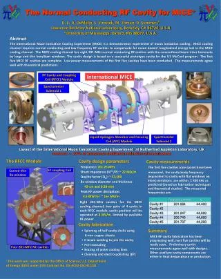
ARES Cavity HOM damper (wave guide type) HOM damper (grooved beam pipe type)
Two types of SiC ceramics SiC-A SiC-B Bullet shape SiC ceramics (wave guide type HOM damper) SiC tile (grooved beam pipe type HOM damper) Both SiC ceramics are a-type and sintered at normal pressure. Boron is used as an additive on densification.
is important parameter as well ase” Diameter : 40 mm ¢r : 22 Frequency : 0.7 GHz fc : ~0.9 GHz Diameter : 40 mm ¢r : 22 Frequency : 1.5 GHz fc : ~0.9 GHz Dielectric rod in a parallel plate line. Frequency < fc : HE11 mode propagates outside the rod mainly. Frequency > fc : HE11 mode is propagates inside the rod. Critical frequency (= fc) is a function of e¢ and diameter of the rod. *Y.Takeuchi et al. “The SiC Absorber for the KEKB ARES Cavity”, EPAC 96.
Measurement of permittivity • ¢ • Measured with HP85070B Dielectric Probe Kit+HP8510C Network Analyzer • Frequency range 0.2~10 GHz. 0.1GHz step. • Samples All sintered lots.
Typical Permittivities of the SiC Ceramics SiC-B SiC-A Dielectric relaxation. This curve behavior is like a Debye-type relaxation. Dielectric relaxation ?
Debye Model Input : Step function Output : P0(t)=P0(1-e-t/t) Debye equation (1) where er0=er¢(w=0), er=er¢(w=) t : relaxation time. Debye model is characterized by the three parameters, er0, erand t.
Cole-Cole Diagram • Horizontal axis : er • Vertical axis : er Locus ( Debye model) half circle
Cole-Cole Diagram of SiC-A and SiC-B • SiC-B Debye type Dielectric Relaxation
Three Parameters of Debye Model (SiC-B) er0 = 85.7 er= 13.6 t= 2.55 x10⁻¹⁰ (sec)
Schematic Model of SiC Ceramics with BeO Addition Grain boundary Grain : P-Type Semiconductor (r<10 W·cm) Carrier Depletion Layer (High Electric Insulation) Resistivity of SiC Ceramics (BeO addition) is higher than 1013W·cm. * K.Maeda, et al., “Grain-boundary Effect in Highly Resistive SiC Ceramics with High Thermal Conductivity”, pp. 260-268 in Advances in Ceramics, Vol. 7, Additives and Interfaces in Electronic Ceramics, ed. M.F.Yan and A.H.Heuer, American Ceramics Society, Columbus, OH., 1984.
Two-layer Model and Equivalent Circuit K. Maeda et al. (Hitachi co.) predicted dielectric properties of SiC ceramics using this equivalent circuit in 1985. * K.Maeda, et al., “Dielectric Behavior of SiC Ceramics with BeO Addition”, Extended Abstract of Electronics Div. 21-E-85, Annual Meeting, Am. Ceram. Soc., 1985.
Probably, SiC-B has a Similar Grain Structure Grain : P-type Semiconductor (Boron is doped r«10 W·cm ) rBoron doped) < rBeO doped) * Resistivity of SiC-B is about 2x10⁵W·cm. rAl doped) < rB doped) < rBeO doped) * • Y.Takeda et al. “Effects of Additives on Thermal Conductivity and Electrical Resistivity of SiC Ceramics”, Yogyo Kyokai-shi 95, [9],1987. • Ceramic Society of Japan.
Effective Permittivity (SiC-B) Calculated from Equivalent Circuit Effective permittivity (2-1) (2-2) where s is coductivity, t = RgRd(Cg+Cd)/(Rg+Rd) Rg«Rd, Cg«CdRgCd < 0.05 above 0.2GHz. negligibly small (2-1) and (2-2) Debye equations.
he e at lower frequencies is predicted by the model. Permittivity (SiC-B) vs Frequency Calculated from Equation (2-1) and (2-2). Debye parameters( er0, er and t ) form the measurement data are used. Permittivity (SiC-B) vs Frequency Measured data he e at lower frequency ( < 0.2GHz ) should be confirmed.
Conclusions • Dielectric properties of SiC-B are explained by the structure of the grain and grain boundary. • We can probably control the dielectric constant of SiC ceramics by using additives. • We will use these results for the next future plan “Super KEKB”. Thank you.