Mixed Signal VLSI
160 likes | 933 Vues
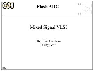
Mixed Signal VLSI. Dr. Chris Hutchens Xunyu Zhu. Outline. Introduction to the flash ADC structure The challenges of high-speed flash ADC applications. Flash ADC Block Diagram. The Comparator is Key. Preamplifier. Regenerator. The schematic of comparator.

Mixed Signal VLSI
E N D
Presentation Transcript
Mixed Signal VLSI Dr. Chris Hutchens Xunyu Zhu
Outline Introduction to the flash ADC structure The challenges of high-speed flash ADC applications
The Comparator is Key Preamplifier Regenerator The schematic of comparator Preamplifier buffering or isolation from the regenerator: • To minimize large sign kickback/flashback effect. • Preamplifier can be set low gain to work at high frequency. Switches are an alternate choice.
Bubble Detector/Filter Features • Error correction ability
Tradeoff Speed-power-accuracy tradeoff The relationship between the speed, power, and accuracy for a Flash ADC is given by [2], where, Avt is the Pelgrom process-dependent parameter(s). From above it is shown that without extra precautions (topology),technology scaling increases the power consumption. Two at the architectural level [2]: • analog processing techniques (for example: folding interpolating) • averaging techniques - reduces the offset specification for high-speed ADC without requiring larger transistors areas Both decreases input capacitance and number of preamplifiers or comparators..
Challenges Input Capacitive loading Resistor String Bowing Signal and Clock Delay
Challenges Input Capacitive Loading • The larger capacitance at the input- the lower the input frequency and increase the power consumption. • The higher the n, the larger number of comparators. • Larger n demands smaller offset voltage at the input node- requires larger transistor, and larger Cgs, [1]. The high bandwidth GBP. GBP=gm/CL, Keep the ΔV constant, in order to get larger GBP, larger transistor needed to get larger gm. Solution: Reducing the large capacitive loading, interpolating and averaging techniques will be adopted.
Challenges The restriction for Cgs: • Input signal loss error The small-signal model of preamplifier The schematic of preamplifier Offset voltage Where the Aβ is process-related constant
Challenges Possible transfer responses for the input-comparator output signals, V1 and V2, and their interpolated signals After interpolating, the maximum offset is not change 4-bit interpolating A/D converter (interpolating factor of 4)
Challenges Averaging architecture [3] It works as following: An array of differential pairs injects two different types of stimuli currents into the averaging network. First, the differential signal currents ΔIs(n) limited by the linear region of the differential pair, enter the network. Second, “noise” currents ΔIos(n) due to the transistor random mismatches also enter the averaging network. A well designed averaging network should filter out the random currents without losing the signal currents. Offset averaging as spatial filtering Optimum averaging network lowers random offset by up to 3 times – 9 amps in the linear region. • Accuracy is maintained with 9 times smaller FETs than if no averaging used. • 9 times less capacitance – possible and reduced power consuption. • With same bias current –i.e. gm is 3X due to 3X Veff bandwidth is 3 times larger [4].
Challenges • Resistor String Bowing Originally, bowing was observed in bipolar applications • Input currents of the bipolar comparators cause errors on the voltages of the nodes of the resistor string. • In CMOS applications the bowing occurs at high frequencies. Vreference The small-signal model of preamplifier The schematic of preamplifier
Challenges Signal and Clock Delay • Even very small differences in the clock or signal arrival at the different comparators inputs results in errors. • Routing differences • capacitive loading • Jitter. At 300 MHz and 12 bits Where f is the input signal frequency A is the amplitude of the input signal n is the number of ADC resolution bits c is the velocity of the light εr is the relative electric permittivity Solution: The clock and signals(s) should such that all delays matched. Signals delays do not need to match clock delays. The exception being pipelined and interleaved ADCs.
Challenges Design Methodology Given Inputs – Number of bits, sampling rate (fn), Pellgrom numbers, noise models, KP, Lambda effective, and parasitic Cs. • Estimate required Ws – Differential Pair and Regenerator • Using Pellgrom numbers and Noise models • Using required C – noise models and/or charge injection errors find gm and W from fn Select the greater Ws and estimate power consumption. If not satisfied with the power consumption or bandwidth. Elect to use averaging or interpolation or both. Design an averaging amplifier that keeps eight or more amplifiers in the linear region. With 8 in the linear region one can reduce the area by 9X and the power or increase the BW by 3X as well several combinations in between.
Reference [1] M.J.M Pelgrom, A.C.J. Duinmaijer, and A.P.G. Welbers, “Matching properties of MOS transistor”, IEEE J. Solid-State Circuits, vol. 24, pp.1433-1440, Oct. 1989. [2] Koen Uyttenhove, M. Steyaert, “Speed-Power-Accuracy Tradoff in high-speed CMOS ADCs”, IEEE trans. Circuit and Systems-II, vol.49, No.4, Apr. 2002. [3] H. Pan, M. Segami, M. Choi, J. Cao, and A. A. Abidi, “A 3.3V 12-b 50-MS/s A/D converter in 0.6um CMOS with over 80dB SFDR,” IEEE J. Solid-State Circuits, vol. 35, pp. 1769-1780, Dec. 2000. [4] M. Choi, and A. A. Abidi, “A 6-b 1.3-Gsample/s A/D Converter in 0.35um CMOS,” IEEE J. Solid-State Circuits, vol 36, Dec. 2001.