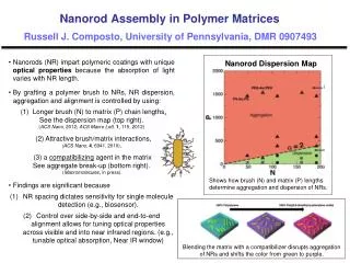
Dynamic Dispersion Compensator
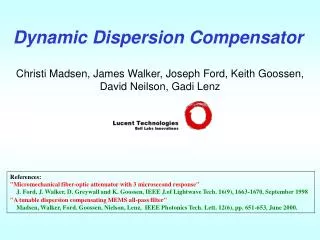
Dynamic Dispersion Compensator. Christi Madsen, James Walker, Joseph Ford, Keith Goossen, David Neilson, Gadi Lenz. References: "Micromechanical fiber-optic attenuator with 3 microsecond response"

Dynamic Dispersion Compensator
E N D
Presentation Transcript
Dynamic Dispersion Compensator Christi Madsen, James Walker, Joseph Ford, Keith Goossen, David Neilson, Gadi Lenz References: "Micromechanical fiber-optic attenuator with 3 microsecond response" J. Ford, J. Walker, D. Greywall and K. Goossen, IEEE J.of Lightwave Tech. 16(9), 1663-1670, September 1998 "A tunable dispersion compensating MEMS all-pass filter" Madsen, Walker, Ford. Goossen, Nielson, Lenz, IEEE Photonics Tech. Lett. 12(6), pp. 651-653, June 2000.
Fiber core index depends (slightly) on l Any modulated signal has nonzero linewidth Chromatic dispersion is the result: Spread in arrival time after signal transmission Fiber core index depends (slightly) on l Any modulated signal has nonzero linewidth Chromatic dispersion is the result: Spread in arrival time after signal transmission 100 km 1 km 500 km 1500 km Fiber spans are “dispersion compensated” But residual dispersion at 3000 km D = 1050 ps/nm V. Srikant (Corning) OFC 2001 DCF DCF DCF DCF DCF Is that OK? Depends on data rate B and length L: (relation for 1 dB power penalty; Tigye Li, Proc. IEEE, 1993) B2DL ~ 105 ps/nm (Gb/s2) MARGINAL Cumulative dispersion budget: 1000 ps/nm @ 10 Gb/s 63 ps/nm @ 40 Gb/s CRITICAL Chromatic dispersion in long-distance telecom
Equalizer Dispersion Compensator I BER feedback Uncompensated Compensated Dynamic chromatic dispersion compensation
Gires-Tournois Interferometer Periodic spectral phase response L / 2 Round Trip Delay Free Spectral Range Phase-only “all-pass” filter • For a lossless filter, magnitude response = 1 (allpass!) • Periodic Gaussian dispersion feature (DCF requires linear chirp) • Approximately linear dispersion over a limited bandwidth Madsen, Walker, Ford, Goossen & Lenz, ECOC 1999; see also recent IEEE LEOS article
1 2 3 4 Increases passband width and total dispersion Ripple = dev. from ideal linear response Multi-stage Filter Dispersion Madsen, Walker, Ford, Goossen & Lenz, ECOC 1999
Voltage Response measured theory input input reflect reflect Vdrive l/4 SiNx l/4 SiNx PSG PSG Drive voltage (V) Silicon Silicon transmit transmit 0 < Vdrive < 30V 3l/4 < gap < l/2 0 < Vdrive < 30V 3l/4 < gap < l/2 Vdrive The “MARS” resonant MEMS modulator MARS (Membrane Anti-Reflection Switch) analog optical modulator l/4 Silicon Nitride “drumhead” suspended over a Silicon substrate Ford, Walker, Greywall & Goossen, IEEE J. Lightwave Tech. 16, 1998 Greywall, Busch & Walker, Sensors & Actuators A A72, 1999. Goossen, Arney & Walker, IEEE Phot. Tech. Lett. 6, 1994
£ £ 0 R 70% L/2 2 = r R 100%Reflector (dielectric enhanced gold mirror) Tunable Partial Reflector V Substrate MARS All-Pass Filter Double polysilicon MEMS structure (flat l response, no charging) 411 um thick Silicon (100 GHz FSR) 2 control parameters per stage: MEMS voltage controls front mirror reflectivity (phase feature amplitude) Substrate temperature controls free spectral range (phase feature location) Madsen, Walker, Ford Goossen, Neilson & Lenz, IEEE Phot. Tech. Lett. 12, 2000
optical breadboard package Vmirror TTEC controller input d $ D f f output ferrule collimator device hermetic MEMS VOA package Fiber-coupling package Key optical package parameters Lens focal length f = 3 mm Fiber separation d = 125 um Illuminated diameter D = 600 um MEMS device diameter 1250 um Substrate thickness t = 411 um Package loss (mirror at device plane) 0.4 dB
Awindow-Afeatures Awindow Scatter = ( )N Cavity round-trip loss Absorption = (e-aL)N a = 10-4/cm Reflection = (Rmirror)N device R = 98.5% T = 99.3% Shift = 10-0.434(NdT/nF)2 Dy = 5 / 600 um Defocus = f(Nf) package fmembrane< 444 mm (20 um / pass) Coupling = To T = 93.3%
1 Measured Phase & Amplitude Wideband (30 nm) Transmission Single filter response Madsen, Walker, Ford Goossen, Neilson & Lenz, IEEE Phot. Tech. Lett. 12, 2000
Tuned for 50 GHz bandwidth and 100 GHz (0.8 nm) FSR 1 2 Negative Positive Madsen, Walker, Ford Goossen, Neilson & Lenz, IEEE Phot. Tech. Lett. 12, 2000 2-stage DCF results Design: Dispersion goal = +/-104 ps/nm; predicted ripple of +/- 2.5 ps Result: Set at +/- 102 ps/nm, yielded ripple of +/- 2.5 ps
2x dispersion for 30 GHz bandwidth and 100 GHz (0.8 nm) FSR 1 2 Madsen, Walker, Ford Goossen, Neilson & Lenz, IEEE Phot. Tech. Lett. 12, 2000 2-stage DCF results (continued) 200 ps/nm range, 1.5 ps ripple (further improvement in loss uniformity required)
Current status: Still R&D! Optical performance (loss uniformity) needs to be improved Control algorithms need more development Dispersion compensation not critical until 40 Gb/s deployed