Key Components and Layers of a PCB Explained
0 likes | 10 Vues
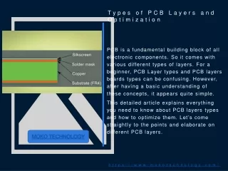
A Printed Circuit Board (PCB) is a crucial component in modern electronics, enabling the connection and operation of various electrical components. It consists of multiple layers, including the substrate, copper traces, solder mask, and silkscreen, each serving a unique function. The substrate provides structural support, while copper traces facilitate signal transmission. The solder mask protects the copper from oxidation and prevents short circuits, and the silkscreen aids in assembly by marking component locations. Designed with precision, often using professional PCB Design Services, a PCB

Key Components and Layers of a PCB Explained
E N D
Presentation Transcript
Key Components and Layers of a PCB Explained
Introduction A PCB consists of multiple layers and components that work together to facilitate electrical connectivity and mechanical support. Each layer plays a specific role in the overall functionality of the board. The combination of conductive and insulating layers forms a complex structure that ensures precise signal transmission while maintaining the integrity of the device.
Key Components of a PCB 1. Substrate The substrate forms the base of the PCB and provides mechanical support. Typically made from materials like fiberglass (FR-4), it ensures rigidity and dimensional stability. Substrate selection is a critical aspect of PCB Design Services, as it influences the board's thermal and electrical properties. 2. Conductive Tracks These thin, copper-based tracks connect various components on the board. Their layout, determined during the PCB Layout Services phase, ensures signal integrity and minimizes electrical interference.
Understanding the Layers of a PCB PCBs can range from simple single-layer boards to complex multi-layer designs, depending on the application's requirements. Each layer in a PCB serves a specific purpose, and its design is optimized using advanced PCB Layout Services. 1. Top and Bottom Layers The outermost layers of a PCB house the conductive traces and components. These layers are essential for establishing connections and are often designed with high precision using PCB Design Services. 2. Inner Layers In multi-layer PCBs, inner layers are dedicated to power distribution and signal routing. These layers are insulated from one another and are crucial for managing complex circuits.
The Role of PCB Design Services PCB Design Services ensure that every layer and component is precisely planned to meet specific performance requirements. By leveraging advanced software tools, designers can create layouts that optimize signal flow, reduce interference, and ensure manufacturability. These services are particularly important for complex multi-layer boards, where the placement of each trace and via must be meticulously calculated.
The Importance of PCB Layout Services The design of a PCB is only as good as its layout. PCB Layout Services focus on the physical arrangement of components, traces, and layers to achieve maximum efficiency. This process involves considering factors such as heat dissipation, signal integrity, and electromagnetic compatibility. A well-executed layout minimizes errors during manufacturing and enhances the overall performance of the board.
Conclusion Understanding the components and layers of a PCB is essential to recognizing the intricate processes involved in its design and production. By utilizing professional PCB Design Services, manufacturers can develop reliable and high-performance PCBs tailored to the demands of modern technology. Whether for consumer electronics or industrial applications, a thoughtfully designed PCB serves as the foundation of innovation and functionality.