Download
1 / 60
670 likes | 1.74k Vues
CHAPTER 11 Semiconductor Theory and Devices. 11.1 Band Theory of Solids 11.2 Semiconductor Theory 11.3 Semiconductor Devices 11.4 Nanotechnology.

E N D
CHAPTER 11Semiconductor Theory and Devices • 11.1 Band Theory of Solids • 11.2 Semiconductor Theory • 11.3 Semiconductor Devices • 11.4 Nanotechnology It is evident that many years of research by a great many people, both before and after the discovery of the transistor effect, has been required to bring our knowledge of semiconductors to its present development. We were fortunate to be involved at a particularly opportune time and to add another small step in the control of Nature for the benefit of mankind. - John Bardeen, 1956 Nobel lecture
11.1: Band Theory of Solids • In Chapter 10 you learned about structural, thermal, and magnetic properties of solids. In this chapter we concentrate on electrical conduction.
Categories of Solids • There are three categories of solids, based on their conducting properties: • conductors • semiconductors • insulators
0 Electrical Resistivity and Conductivity of Selected Materials at 293 K
Reviewing the previous table reveals that: • The electrical conductivity at room temperature is quite different for each of these three kinds of solids • Metals and alloys have the highest conductivities • followed by semiconductors • and then by insulators
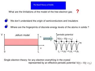
Semiconductor Conduction • The free-electron model from Chapter 9 does not apply to semiconductors and insulators, since these materials simply lack enough free electrons to conduct in a free-electron mode. There is a different conduction mechanism for semiconductors than for normal conductors.
Resistivity vs. Temperature Figure 11.1: (a) Resistivity versus temperature for a typical conductor. Notice the linear rise in resistivity with increasing temperature at all but very low temperatures. (b) Resistivity versus temperature for a typical conductor at very low temperatures. Notice that the curve flattens and approaches a nonzero resistance as T→ 0. (c) Resistivity versus temperature for a typical semiconductor. The resistivity increases dramatically as T → 0.
Band Theory of Solids • In order to account for decreasing resistivitywith increasing temperature as well as other properties of semiconductors, a new theory known as the band theory is introduced. • The essential feature of the band theory is that the allowed energy states for electrons are nearly continuous over certain ranges, called energy bands, with forbidden energy gaps between the bands.
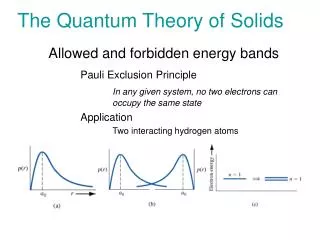
Band Theory of Solids • Consider initially the known wave functions of two hydrogen atoms far enough apart so that they do not interact.
Interaction of the wave functions occurs as the atoms get closer: An atom in the symmetric state has a nonzero probability of being halfway between the two atoms, while an electron in the antisymmetric state has a zero probability of being at that location. Band Theory of Solids Symmetric Antisymmetric
In the symmetric case the binding energy is slightly stronger resulting in a lower energy state. Thus there is a splitting of all possible energy levels (1s, 2s, and so on). When more atoms are added (as in a real solid), there is a further splitting of energy levels. With a large number of atoms, the levels are split into nearly continuous energy bands, with each band consisting of a number of closely spaced energy levels. Band Theory of Solids
Kronig-Penney Model • An effective way to understand the energy gap in semiconductors is to model the interaction between the electrons and the lattice of atoms. • R. de L. Kronig and W. G. Penney developed a useful one-dimensional model of the electron lattice interaction in 1931.
Kronig and Penney assumed that an electron experiences an infinite one-dimensional array of finite potential wells. Each potential well models attraction to an atom in the lattice, so the size of the wells must correspond roughly to the lattice spacing. Kronig-Penney Model
Since the electrons are not free their energies are less than the height V0 of each of the potentials, but the electron is essentially free in the gap 0 < x <a, where it has a wave function of the form where the wave number k is given by the usual relation: Kronig-Penney Model
Tunneling • In the region between a < x < a + b the electron can tunnel through and the wave function loses its oscillatory solution and becomes exponential:
Matching solutions at the boundary, Kronig and Penney find Here K is another wave number. Kronig-Penney Model
The left-hand side is limited to values between +1 and −1 for all values of K. Plotting this it is observed there exist restricted (shaded) forbidden zones for solutions. Kronig-Penney Model
The Forbidden Zones Figure 11.5 (a) Plot of the left side of Equation (11.3) versus ka for κ2ba / 2 = 3π / 2. Allowed energy values must correspond to the values of k for for which the plotted function lies between -1 and +1. Forbidden values are shaded in light blue. (b) The corresponding plot of energy versus ka for κ2ba / 2 = 3π / 2, showing the forbidden energy zones (gaps).
Important differences between the Kronig-Penney model and the single potential well • For an infinite lattice the allowed energies within each band are continuous rather than discrete. In a real crystal the lattice is not infinite, but even if chains are thousands of atoms long, the allowed energies are nearly continuous. • In a real three-dimensional crystal it is appropriate to speak of a wave vector. The allowed ranges for constitute what are referred to in solid state theory as Brillouin zones.
And… • In a real crystal the potential function is more complicated than the Kronig-Penney squares. Thus, the energy gaps are by no means uniform in size. The gap sizes may be changed by the introduction of impurities or imperfections of the lattice. • These facts concerning the energy gaps are of paramount importance in understanding the electronic behavior of semiconductors.
Band Theory and Conductivity • Band theory helps us understand what makes a conductor, insulator, or semiconductor. • Good conductors like copper can be understood using the free electron • It is also possible to make a conductor using a material with its highest band filled, in which case no electron in that band can be considered free. • If this filled band overlaps with the next higher band, however (so that effectively there is no gap between these two bands) then an applied electric field can make an electron from the filled band jump to the higher level. • This allows conduction to take place, although typically with slightly higher resistance than in normal metals. Such materials are known as semimetals.
Valence and Conduction Bands • The band structures of insulators and semiconductors resemble each other qualitatively. Normally there exists in both insulators and semiconductors a filled energy band (referred to as the valence band) separated from the next higher band (referred to as the conduction band) by an energy gap. • If this gap is at least several electron volts, the material is an insulator. It is too difficult for an applied field to overcome that large an energy gap, and thermal excitations lack the energy to promote sufficient numbers of electrons to the conduction band.
Smaller energy gaps create semiconductors • For energy gaps smaller than about 1 electron volt, it is possible for enough electrons to be excited thermally into the conduction band, so that an applied electric field can produce a modest current. The result is a semiconductor.
11.2: Semiconductor Theory • At T = 0 we expect all of the atoms in a solid to be in the ground state. The distribution of electrons (fermions) at the various energy levels is governed by the Fermi-Dirac distribution of Equation (9.34): β = (kT)−1 and EF is the Fermi energy.
Temperature and Resistivity • When the temperature is increased from T = 0, more and more atoms are found in excited states. • The increased number of electrons in excited states explains the temperature dependence of the resistivity of semiconductors. Only those electrons that have jumped from the valence band to the conduction band are available to participate in the conduction process in a semiconductor. More and more electrons are found in the conduction band as the temperature is increased, and the resistivity of the semiconductor therefore decreases.
Some Observations • Although it is not possible to use the Fermi-Dirac factor to derive an exact expression for the resistivity of a semiconductor as a function of temperature, some observations follow: • The energy E in the exponential factor makes it clear why the band gap is so crucial. An increase in the band gap by a factor of 10 (say from 1 eV to 10 eV) will, for a given temperature, increase the value of exp(βE) by a factor of exp(9βE). • This generally makes the factor FFD so small that the material has to be an insulator. • Based on this analysis, the resistance of a semiconductor is expected to decrease exponentially with increasing temperature. • This is approximately true—although not exactly, because the function FFD is not a simple exponential, and because the band gap does vary somewhat with temperature.
Clement-Quinnell Equation • A useful empirical expression developed by Clement and Quinnell for the temperature variation of standard carbon resistors is given by where A, B, and K are constants.
Test of the Clement-Quinnell Equation Figure 11.7: (a) An experimental test of the Clement-Quinnell equation, using resistance versus temperature data for four standard carbon resistors. The fit is quite good up to 1 / T≈ 0.6, corresponding to T ≈ 1.6 K. (b) Resistance versus temperature curves for some thermometers used in research. A-B is an Allen-Bradley carbon resistor of the type used to produce the curves in (a). Speer is a carbon resistor, and CG is a carbon-glass resistor. Ge 100 and 1000 are germanium resistors. From G. White, Experimental Techniques in Low Temperature Physics, Oxford: Oxford University Press (1979).
Holes and Intrinsic Semiconductors • When electrons move into the conduction band, they leave behind vacancies in the valence band. These vacancies are called holes. Because holes represent the absence of negative charges, it is useful to think of them as positive charges. • Whereas the electrons move in a direction opposite to the applied electric field, the holes move in the direction of the electric field. • A semiconductor in which there is a balance between the number of electrons in the conduction band and the number of holes in the valence band is called an intrinsic semiconductor. Examples of intrinsic semiconductors include pure carbon and germanium.
Impurity Semiconductor • It is possible to fine-tune a semiconductor’s properties by adding a small amount of another material, called a dopant, to the semiconductor creating what is a called an impurity semiconductor. • As an example, silicon has four electrons in its outermost shell (this corresponds to the valence band) and arsenic has five. Thus while four of arsenic’s outer-shell electrons participate in covalent bonding with its nearest neighbors (just as another silicon atom would), the fifth electron is very weakly bound. It takes only about 0.05 eV to move this extra electron into the conduction band. • The effect is that adding only a small amount of arsenic to silicon greatly increases the electrical conductivity.
n-type Semiconductor • The addition of arsenic to silicon creates what is known as an n-type semiconductor (n for negative), because it is the electrons close to the conduction band that will eventually carry electrical current. The new arsenic energy levels just below the conduction band are called donor levels because an electron there is easily donated to the conduction band.
Acceptor Levels • Consider what happens when indium is added to silicon. • Indium has one less electron in its outer shell than silicon. The result is one extra hole per indium atom. The existence of these holes creates extra energy levels just above the valence band, because it takes relatively little energy to move another electron into a hole • Those new indium levels are called acceptor levels because they can easily accept an electron from the valence band. Again, the result is an increased flow of current (or, equivalently, lower electrical resistance) as the electrons move to fill holes under an applied electric field • It is always easier to think in terms of the flow of positive charges (holes) in the direction of the applied field, so we call this a p-type semiconductor (p for positive). • acceptor levels p-Type semiconductors • In addition to intrinsic and impurity semiconductors, there are many compound semiconductors, which consist of equal numbers of two kinds of atoms.
Thermoelectric Effect • In one dimension the induced electric field E in a semiconductor is proportional to the temperature gradient, so that where Q is called the thermoelectric power. • The direction of the induced field depends on whether the semiconductor is p-type or n-type, so the thermoelectric effect can be used to determine the extent to which n- or p-type carriers dominate in a complex system.
Thermoelectric Effect • When there is a temperature gradient in a thermoelectric material, an electric field appears. • This happens in a pure metal since we can assume the system acts as a gas of free electrons. • As in an ideal gas, the density of free electrons is greater at the colder end of the wire, and therefore the electrical potential should be higher at the warmer end and lower at the colder end. • The free-electron model is not valid for semiconductors; nevertheless, the conducting properties of a semiconductor are temperature dependent, as we have seen, and therefore it is reasonable to believe that semiconductors should exhibit a thermoelectric effect. • This thermoelectric effect is sometimes called the Seebeck effect.
The Thomson and Peltier Effects • In a normal conductor, heat is generated at the rate of I2R. But a temperature gradient across the conductor causes additional heat to be generated. This is the Thomson Effect. Here heat is generated if current flows toward the higher temperature and absorbed if toward the lower. • The Peltier effect occurs when heat is generated at a junction between two conductors as current passes through the junction.
The Thermocouple • An important application of the Seebeck thermoelectric effect is in thermometry. The thermoelectric power of a given conductor varies as a function of temperature, and the variation can be quite different for two different conductors. This difference makes possible the operation of a thermocouple.
11.3: Semiconductor Devices pn-junction Diodes • Here p-type and n-type semiconductors are joined together. • The principal characteristic of a pn-junction diode is that it allows current to flow easily in one direction but hardly at all in the other direction. We call these situations forward bias and reverse bias, respectively.
Operation of a pn-junction Diode Figure 11.12: The operation of a pn-junction diode. (a) This is the no-bias case. The small thermal electron current (It) is offset by the electron recombination current (Ir). The net positive current (Inet) is zero. (b) With a DC voltage applied as shown, the diode is in reverse bias. Now Ir is slightly less than It. Thus there is a small net flow of electrons from p to n and positive current from n to p. (c) Here the diode is in forward bias. Because current can readily flow from p to n, Ir can be much greater than It. [Note: In each case, It and Ir are electron (negative) currents, but Inet indicates positive current.]
Bridge Rectifiers • The diode is an important tool in many kinds of electrical circuits. As an example, consider the bridge rectifier circuit shown in Figure 11.14. The bridge rectifier is set up so that it allows current to flow in only one direction through the resistor R when an alternating current supply is placed across the bridge. The current through the resistor is then a rectified sine wave of the form • This is the first step in changing alternating current to direct current. The design of a power supply can be completed by adding capacitors and resistors in appropriate proportions. This is an important application, because direct current is needed in many devices and the current that we get from our wall sockets is alternating current. Figure 11.14: Circuit diagram for a diode bridge rectifier. (11.10)
Zener Diodes • The Zener diode is made to operate under reverse bias once a sufficiently high voltage has been reached. The I-V curve of a Zener diode is shown in Figure 11.15. Notice that under reverse bias and low voltage the current assumes a low negative value, just as in a normal pn-junction diode. But when a sufficiently large reverse bias voltage is reached, the current increases at a very high rate. Figure 11.16: A Zener diode reference circuit. Figure 11.15: A typical I-V curve for a Zener diode.
Light Emitting Diodes • Another important kind of diode is the light-emitting diode (LED). Whenever an electron makes a transition from the conduction band to the valence band (effectively recombining the electron and hole) there is a release of energy in the form of a photon (Figure 11.17). In some materials the energy levels are spaced so that the photon is in the visible part of the spectrum. In that case, the continuous flow of current through the LED results in a continuous stream of nearly monochromatic light. Figure 11.17: Schematic of an LED. A photon is released as an electron falls from the conduction band to the valence band. The band gap may be large enough that the photon will be in the visible portion of the spectrum.
Photovoltaic Cells • An exciting application closely related to the LED is the solar cell, also known as the photovoltaic cell. Simply put, a solar cell takes incoming light energy and turns it into electrical energy. A good way to think of the solar cell is to consider the LED in reverse (Figure 11.18). A pn-junction diode can absorb a photon of solar radiation by having an electron make a transition from the valence band to the conduction band. In doing so, both a conducting electron and a hole have been created. If a circuit is connected to the pn junction, the holes and electrons will move so as to create an electric current, with positive current flowing from the p side to the n side. Even though the efficiency of most solar cells is low, their widespread use could potentially generate significant amounts of electricity. Remember that the “solar constant” (the energy per unit area of solar radiation reaching the Earth) is over 1400 W/m2, and more than half of this makes it through the atmosphere to the Earth’s surface. There has been tremendous progress in recent years toward making solar cells more efficient. Figure 11.18: (a) Schematic of a photovoltaic cell. Note the similarity to Figure 11.17. (b) A schematic showing more of the working parts of a real photovoltaic cell. From H. M. Hubbard, Science 244, 297-303 (21 April 1989).
Transistors • Another use of semiconductor technology is in the fabrication of transistors, devices that amplify voltages or currents in many kinds of circuits. The first transistor was developed in 1948 by John Bardeen, William Shockley, and Walter Brattain (Nobel Prize, 1956). As an example we consider an npn-junction transistor, which consists of a thin layer of p-type semiconductor sandwiched between two n-type semiconductors. The three terminals (one on each semiconducting material) are known as the collector, emitter, and base. A good way of thinking of the operation of the npn-junction transistor is to think of two pn-junction diodes back to back. Figure 11.22: (a) In the npn transistor, the base is a p-type material, and the emitter and collector are n-type. (b) The two-diode model of the npn transistor. (c) The npn transistor symbol used in circuit diagrams. (d) The pnp transistor symbol used in circuit diagrams.
Transistors • Consider now the npn junction in the circuit shown in Figure 11.23a. If the emitter is more heavily doped than the base, then there is a heavy flow of electrons from left to right into the base. The base is made thin enough so that virtually all of those electrons can pass through the collector and into the output portion of the circuit. As a result the output current is a very high fraction of the input current. The key now is to look at the input and output voltages. Because the base-collector combination is essentially a diode connected in reverse bias, the voltage on the output side can be made higher than the voltage on the input side. Recall that the output and input currents are comparable, so the resulting output power (current × voltage) is much higher than the input power. Figure 11.23: (a) The npn transistor in a voltage amplifier circuit. (b) The circuit has been modified to put the input between base and ground, thus making a current amplifier. (c) The same circuit as in (b) using the transistor circuit symbol.
Field Effect Transistors (FET) • The three terminals of the FET are known as the drain, source, and gate, and these correspond to the collector, emitter, and base, respectively, of a bipolar transistor. Figure 11.25: (a) A schematic of a FET. The two gate regions are connected internally. (b) The circuit symbol for the FET, assuming the source-to-drain channel is of n-type material and the gate is p-type. If the channel is p-type and the gate n-type, then the arrow is reversed. (c) An amplifier circuit containing a FET.
Schottky Barriers • Here a direct contact is made between a metal and a semiconductor. If the semiconductor is n-type, electrons from it tend to migrate into the metal, leaving a depleted region within the semiconductor. This will happen as long as the work function of the metal is higher (or lower, in the case of a p-type semiconductor) than that of the semiconductor. • The width of the depleted region depends on the properties of the particular metal and semiconductor being used, but it is typically on the order of microns. The I-V characteristics of the Schottky barrier are similar to those of the pn-junction diode. When a p-type semiconductor is used, the behavior is similar but the depletion region has a deficit of holes.
Schottky Barriers Figure 11.26: (a) Schematic drawing of a typical Schottky-barrier FET. (b) Gain versus frequency for two different substrate materials, Si and GaAs. From D. A. Fraser, Physics of Semiconductor Devices, Oxford: Clarendon Press (1979).
Semiconductor Lasers • Like the gas lasers described in Section 10.2, semiconductor lasers operate using population inversion—an artificially high number of electrons in excited states • In a semiconductor laser, the band gap determines the energy difference between the excited state and the ground state • Semiconductor lasers use injection pumping, where a large forward current is passed through a diode creating electron-hole pairs, with electrons in the conduction band and holes in the valence band. A photon is emitted when an electron falls back to the valence band to recombine with the hole.
Since their development, semiconductor lasers have been used in a number of applications, most notably in fiber-optics communication. One advantage of using semiconductor lasers in this application is their small size with dimensions typically on the order of 10−4 m. Being solid-state devices, they are more robust than gas-filled tubes. Semiconductor Lasers
Integrated Circuits • The most important use of all these semiconductor devices today is not in discrete components, but rather in integrated circuits called chips. • Some integrated circuits contain a million or more components such as resistors, capacitors, and transistors. • Two benefits:miniaturization and processing speed.