Download
1 / 49
510 likes | 1.9k Vues
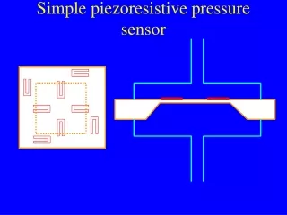
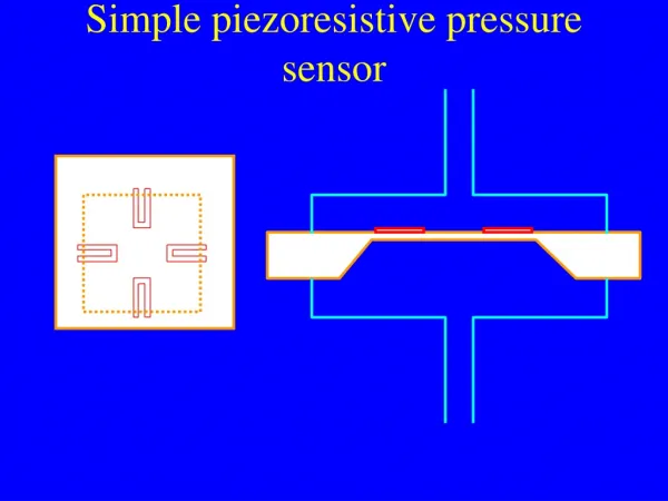
Simple piezoresistive pressure sensor. Simple piezoresistive accelerometer. Simple capacitive accelerometer. Cap wafer may be micromachined silicon, pyrex, … Serves as over-range protection, and damping Typically would have a bottom cap as well. C(x)=C(x(a)). Cap wafer.

E N D
Simple capacitive accelerometer • Cap wafer may be micromachined silicon, pyrex, … • Serves as over-range protection, and damping • Typically would have a bottom cap as well. C(x)=C(x(a)) Cap wafer
Simple capacitive pressure sensor C(x)=C(x(P))
ADXL50 Accelerometer • +-50g • Polysilicon MEMS & BiCMOS • 3x3mm die • Integration of electronics!
ADXL50 Sensing Mechanism • Balanced differential capacitor output • Under acceleration, capacitor plates move changing capacitance and hence output voltage • On-chip feedback circuit drives on-chip force-feedback to re-center capacitor plates (improved linearity).
ADXL50 – block diagram • http://www.analog.com/en/mems-and-sensors/imems-accelerometers/products/index.html
Digital Output MEMS Gyroscope Chip Proof Mass SenseCircuit Rotation induces Coriolis acceleration Electrostatic Drive Circuit J. Seeger, X. Jiang, and B. Boser
1mm Drive 0.01Å Sense MEMS Gyroscope Chip J. Seeger, X. Jiang, and B. Boser
Two-Axis Gyro, IMI(Integrated Micro Instruments Inc.)/ADI (fab)
Single chip six-degree-of-freedom inertial measurement unit (uIMU) designed by IMI principals and fabricated by Sandia National Laboratories
Seal ring Landing ring MEMS Gate Microbump Feedthrough Dielectric Beam Drain Beam Source Package Substrate Drain Gate Source Gate Drain Source NEU/ADI/Radant/MAT Microswitches http://www.radantmems.com/radantmems/switchoperation.html Surface Micromachined Post-Process Integration with CMOS 20-100 V Electrostatic Actuation ~100 Micron Size SEM of NEU microswitch MAT Microswitch
Contact Detail Contact End of Switch
Spectrometer cross-section Surface Micromachined Spring System Electrostatic Actuator Plates
Intensity vs. Wavelength l = 575nm FWHM = 30nm RP = 20 l =515 nm FWHM = 25nm RP = 21 l =625nm FWHM = 39nm RP = 16
Packaged Plasma Source Top View Die in Hybrid Package Side View
Fabrication SEM of Interdigitated Capacitor Structure
Optical MEMS Vibration Sensors Uniform cantilever beam Foster Miller - Diaphragm Cantilevered paddle Cantilevered supported diaphragm
Optically interrogated MEMS sensors 55 mm length cantilevered paddle after 7 hours of B.O.E. releasing and lifted up with a 1mm probe (~0.35mm thick, 2mm gap)
Micromachining Ink Jet Nozzles Microtechnology group, TU Berlin
NEMS: TOWARD PHONON COUNTING: Quantum Limit of Heat Flow. Roukes Group Cal Tech Tito
From Ashcroft and Mermin, Solid State Physics.
Other: NSF-Funded NSEC, Center for High-Rate Nanomanufacturing (CHN): High-rate Directed Self-Assembly of Nanoelements Proof of Concept Testbed • Nanotube Memory Device Partner: Nantero first to make memory devices using nanotubes • Properties:nonvolatile, high speed at <3ns, lifetime (>1015 cycles), resistant to heat, cold, magnetism, vibration, and cosmic radiation. Nanotemplate: • Layer of assembled nanostructures transferred to a wafer. Template is intended to be used for thousands of wafers.
Switch Logic, 1996, Zavracky, Northeastern Inverter NOR Gate
Simple Carbon Nanotube Switch Diameter: 1.2 nm Elastic Modulus: 1 TPa Electrostatic Gap: 2 nm Binding Energy to Substrate: 8.7x10⁻²⁰ J/nm Length at which adhesion = restoring force: 16 nm Actuation Voltage at 16 nm = 2 V Resonant frequency at 16 nm = 25 GHz Electric Field = 109 V/m or 107 V/cm + Geom. (F-N tunneling at > 107 V/cm) Stored Mechanical Energy (1/2 k x2 ) = 4 x 10-19 J = 2.5 eV 4 x 10-19 = ½ CV2 gives C = 2 x 10-19 << electrode capacitance! Much more energy stored in local electrodes than switch.