1 / 6

WLCSP Electroless Platting Market

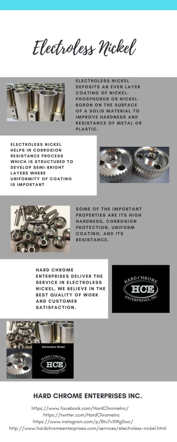
Wafer-Level Chip-Scale Packaging (WLCSP) electroless plating is a process widely used in the semiconductor industry to enhance the functionality and durability of microchips. This technology involves depositing metal layers onto the surface of semiconductor wafers without the need for external electrical power.

Skywalker
Télécharger la présentation

WLCSP Electroless Platting Market

An Image/Link below is provided (as is) to download presentation Download Policy: Content on the Website is provided to you AS IS for your information and personal use and may not be sold / licensed / shared on other websites without getting consent from its author. Content is provided to you AS IS for your information and personal use only. Download presentation by click this link. While downloading, if for some reason you are not able to download a presentation, the publisher may have deleted the file from their server. During download, if you can't get a presentation, the file might be deleted by the publisher.

E N D

Presentation Transcript


More Related