CoE - EE 00142 Computer Organization Set 4 Registers, Datapaths and Operations
620 likes | 1.14k Vues
CoE - EE 00142 Computer Organization Set 4 Registers, Datapaths and Operations. Ron Hoelzeman. Datapaths & Control Units. Datapath Performs data-processing operations Control unit Determines the sequence of those operations. Control signals. ControlUnit. Status signals. Datapath.

CoE - EE 00142 Computer Organization Set 4 Registers, Datapaths and Operations
E N D
Presentation Transcript
CoE - EE 00142Computer OrganizationSet 4Registers, Datapaths and Operations Ron Hoelzeman
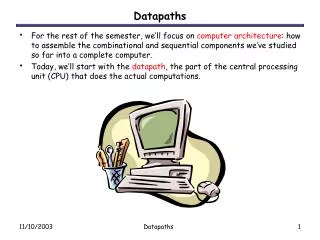
Datapaths & Control Units • Datapath Performs data-processing operations • Control unit Determines the sequence of those operations
Control signals ControlUnit Status signals Datapath Control inputs Control outputs Data inputs Datapath - Control Unit Interaction Data outputs
Signals • Binary signals – one or zero • Control signals Activate data processing operations in proper sequence • Status signals Datapath feedback to control unit
Datapaths • Best defined by registers and operations • Examples: Shift Count Load clear
Register Transfer Operations • Defined by: The set of registers in the system The operations performed on the data stored in the registers The control that supervises the sequence of operations
Registers • Flip Flops Review of basics • Registers Loading Shifting
Registers • Used to store data or instructions • Simply adjacent FF’s with loading and other control logic - gates • Counters are a special case • Sometimes use special names accumulators, program counters, index registers, stack pointer, status register, etc.
R3 R2 R1 R0 R3 R2 R1 R0 Register Remember - just a bundle of Flip-Flops
Input Output Clock D Latch or Flip Flop Triggers on positive edge of clock pulse
Concept of Synchronization Triggers on positive edge of clock pulse Figure 5.2
Concept of Synchronization Because of edge trigger, we can feed the output back around to the input Figure 5.3
4-Bit Register Graphics from: Logic and Computer Design Fundamentals, Mano & Kime, Prentice Hall
4-Bit Register Symbol Graphics from: Logic and Computer Design Fundamentals, Mano & Kime, Prentice Hall
4-Bit Register with Parallel Load Note: When Load =0, the output is connected back to the input because the D-FF does not have a “no change” input condition Graphics from: Logic and Computer Design Fundamentals, Mano & Kime, Prentice Hall
Shift Registers • Logical shift Right or left • Arithmetic shift Right or left • Ring shift
0 R3 R2 R1 R0 Logical Shift Right Examples: 0100 --> 0010 1110 --> 0111
0 R3 R2 R1 R0 Logical Shift Left Examples: 0011 --> 0110 1101 --> 1010
R3 R2 R1 R0 Arithmetic Shift Right • Examples: • Positive numbers 0100 --> 0010 • same as logical shift • Negative numbers 1110 --> 1111 • (-2) --> (-1) not same as logical shift
0 R3 R2 R1 R0 Arithmetic Shift Left • Examples: • Positive numbers 0011 --> 0110 • same as logical shift • Negative numbers 1101 --> 1010 • (-3) --> (-6) same as logical shift
R3 R2 R1 R0 Ring Shift Right Examples: 0101 --> 1010 1110 --> 0111
Shift a variable amount Shift a fixed amount MIPS Shift Instructions
4-Bit Shift Register • On leading edge of clock pulse • Each FF gets output of previous Graphics from: Logic and Computer Design Fundamentals, Mano & Kime, Prentice Hall
4-Bit Shift Register Symbol Graphics from: Logic and Computer Design Fundamentals, Mano & Kime, Prentice Hall
15 8 7 0 PC (H) PC (L) Register Block Diagrams 7 6 5 4 3 2 1 0 15 0 R2
Register Language Examples • PC(L) or PC(7:0) Low order byte of register PC • PC(H) or PC(15:8) High order byte of register PC • R2 R1 Transfer data from R1 to R2
Example Register Transfer Transfer from R1 to R2 when K1 = 1 If (K1 = 1) then (R2 R1) RTL Expression K1:R2 R2
Arithmetic Micro-operations R0 R1 + R2 Addition R2 R2 1’s complement R2 R2 + 1 2’s complement R0 R1 +R2 +1 Subtract R1 R1 +1 Increment R1 R1 – 1 Decrement
Logic Micro-operations R0 R1 Logic NOT R0 R1 R2 Logic AND R0 R1 R2 Logic OR R0 R1 R2 Logic XOR All Bitwise
Logic Examples AND or Mask operation
Logic Examples OR operation
Logic Examples EOR operation Complements selected bits
Shift Micro-operations Before After Shift left R0 sl R0 01110001 11100010 Shift right R0 sr R0 01110001 00111000
Multiplexer-based Transfer If (K1=1) then (R0 R1) else if (K2=1) then (R0 R2) K1: R0 R1,K2: R0 R2
Memory Transfer Memory read: R0 M[AR] Memory write: M[AR] R0 M – Memory – typically RAM AR – Address in memory
Add B to A A Serial Adder • When Shift = 0 • C in = 1 • When Shift = 1 • C in = Clock Figure 5-5 Page 229
0 0 Q 0 D 0 In 0 0 Q D In Shift Load Operation 0 0 Nothing 0 1 Load parallel 1 X Shift Shift Register with Parallel Load 0 0 0 1 0 X Figure 5-6 Page 231
Shift Register - Parallel Load Symbol Graphics from: Logic and Computer Design Fundamentals, Mano & Kime, Prentice Hall
Bidirectional Shift Registerone stage S1 S2 Operation 0 0 NC 0 1 Shift Dn 1 0 Shift Up 1 1 Par Load S1S2 determine which line is connected to the D of Qi Graphics from: Logic and Computer Design Fundamentals, Mano & Kime, Prentice Hall
Register A Register B Add Add/Subtract Unit Sub Accumulator CCR Condition Code Register ALU Block Diagram Normally, the accumulator has logical and arithmetic shift capability, both left and right
Single Bus Example 7-6b Transfer Mechanisms
Note Bidirectional Enable causes output
B selects R3 Destination select G to select A + B A selects R2 Status bits MD select MF select Block Diagram of a Datapath Example R1 R2 + R3 Figure 7-9 Page 328 Graphics from: Logic and Computer Design Fundamentals, Mano & Kime, Prentice Hall
Basics of Fig 7-9 All registers connected to Mux A and Mux B Mux B also has “constant in” select Both Bus A & B have output paths G selects arithmetic operation H select shifting operation Mux F selects output of ALU or shifter Mux D selects what goes back to registers Destination select chooses which register
Sequence of OperationsR1 R2 + R3 A select - R2 onto bus A B select - R3 onto Mux B Mux B select - R3 onto bus B G select - operation of A + B MF select - ALU out to Mux F in MD select - Mux F out to Bus D Destination select - Bus D to R1 Load enable - load R1
Block Diagram of n-Bit ALU Figure 7-10 Page 330 Graphics from: Logic and Computer Design Fundamentals, Mano & Kime, Prentice Hall