Memory Hierarchy
Submitted by: Ajay Kumar Parimi Srinivas Paladi . Memory Hierarchy. What is Memory? Memory is a storage device and it is the part of the computer that holds data and instructions for processing. Each memory location is identified by an address

Memory Hierarchy
E N D
Presentation Transcript
Submitted by: Ajay Kumar Parimi Srinivas Paladi Memory Hierarchy
What is Memory? Memory is a storage device and it is the part of the computer that holds data and instructions for processing. • Each memory location is identified by an address • The Control unit finds data and instructions using this address. Memory Hierarchy
What is Memory Hierarchy? The hierarchical arrangement of data storage or memory in a computer architecture is often referred to as Memory Hierarchy. It is designed to take the advantage over the properties like speed, size, latency and reduce the time it takes to perform an memory related operation.
Before we go any further in to Memory Hierarchy, let us have a simple glance at CPU and its operations. A CPU executes a set of stored instructions. It constitutes 1. Arithmetic and Logic unit (ALU) It performs all arithmetic and logical operations. 2. Control unit (CU) It contains circuitry that uses electrical signals to control the execution of instructions.
Instructions are stored in the memory. Before an instruction can be executed, program instructions and data must be placed into memory from an input device or a secondary storage device. How CPU executes instructions ? The control unit fetches the instruction from memory. The control unit decodes the instruction and directs it to the arithmetic/logic unit with necessary data.
The time to perform these two steps is considered as Instruction time (I-time). The ALU executes the arithmetic or logical instruction, that is it performs the actual operation on the data. The ALU stores the result of this operation in a small memory location also called a Register. The time to perform these two steps is considered as Execution time (E-time). The combination of I-time and E-time is called the machine cycle.
In most computers nowadays the memory is stored in 1. Registers 2. Cache 3. Main Memory 4. Disk storage, tapes, optical disks etc. Let us get more familiar with the storage types before we get in to the hierarchical arrangement.
Registers A register is a small amount of storage location available on the CPU, whose contents can be accessible more quickly than any other storage. Registers are temporary storage areas for instructions or data and work under Control Unit. Registers are used to accept, hold, and transfer instructions or data and Perform arithmetic or logical comparisons at high speed.
Some special registers are as below 1. An accumulator, which collects the result of computations. 2. An address register, which keeps track of where a given instruction or piece of data is stored in memory. 3. A storage register, which temporarily holds data taken from or about to be sent to memory. 4. A general-purpose register, which is used for several functions.
Cache Memory: A cache is a block of memory for temporary storage of data likely to be used again. A cache is a collection of data duplicating original values stored elsewhere or computed earlier . In other words, a cache is a temporary storage area where frequently accessed main memory data can be stored for rapid access. A Cache is used by the CPU to reduce the average time to access the memory.
Keywords in Cache operation: A cache hit in a read/write is accomplished when the tags related to the address location of the main memory matches with that of the cache memory. If no match is found then it is termed as cache miss. A cache miss can be classified mainly in to 3 types:1. Compulsory misses are caused by the first reference to a datum. 2. Capacity misses occur due to the finite size of the cache.
Keywords in Cache operation: Conflict misses are those that could have been avoided, had the cache not forced out an entry earlier. These misses can be further classified as mapping misses, which are unavoidable given a particular amount of associativity. Replacement misses which occur due to particular victim choice of the replacement policy.
A Cache miss on a instruction fetch requires the processor to stall. In other terms it need to wait until the instruction is available from the main memory. For a given miss rate for reads and writes in cache memory, we have Read-stall cycles = Reads * Read miss rate * Read miss penalty Write-stall cycles = (Writes * Write miss rate * Write miss penalty) + Write buffer stalls In most of the cache memory systems the penalties for read and write are almost same, so Memory-stall cycles = memory accesses* Cache miss rate * Cache miss penalty
Keywords in Cache operation: A write-through cache writes the data written in the cache immediately in to the main memory. But its not done instantly as in the case of write-back. So in the case of a cache miss the later needs 2 memory accesses to write the data. A replacement policy are some optimal instructions followed to manage cache of information for a structure. A cache is said to be fully-associative if replacement policy is free to choose any cache entry to hold the copy.
Keywords in Cache operation: Direct-mapped cache fill is one in which each memory block entry in the main memory is mapped only to one location in the cache. The effectiveness of cache memory can be defined in terms of hit rate, which is the proportion of accesses that result in a hit. A write policy controls the timing of the data write in to the main memory.
TLB: Translation lookasidebuffer is a CPU cache that uses memory management hardware to improve the speed of virtual address translation. A TLB has fixed amount of slots containing the page table entries. A page table is one which maps virtual addresses to physical addresses. In a TLB the search key is a virtual address and the search result is a physical address.
TLB references reside between CPU and cache if the cache is addressed virtually. • TLB references reside in between CPU cache and the main memory if the cache is physically addressed. • TLB misses can be handled in 2 ways: • With hardware TLB management. • With software TLB management.
Main Memory: Primary storage is usually referred to as main memory. It is the only memory which is accessible to the CPU. The main memory of the computer is also known as RAM, standing for Random Access Memory. It is constructed from integrated circuits and needs to have electrical power in order to maintain its information. When power is lost, the information is lost too.!!
The main memory is sub divided in to as Processor Registers, where each register typically holds up to 32 to 64 bits of data. A Processor cache is an intermediate stage between registers and the main memory. Its main purpose is to increase the speed and performance of the computer. Types of RAM: 1. Static RAM(SRAM) 2. Dynamic RAM(DRAM) 3. Erasable programmable ROM (EPROM) 4. Electrically erasable PROM (EEPROM
Accessing Main Memory: Data flow between the processor and the main memory is done using the buses. Each transfer of data is often referred to as a Bustransaction. A read transaction transfers data from main memory to the CPU. Each write transaction transfers data from the CPU To the main memory. The basic bus structure that connects the CPU and the main memory is as below: On a load operation by the CPU, address of that particular content is loaded in to the registers.
The bus interface initiates the bus transaction. During a read the CPU places the address on the system bus and is passed to the memory bus via the I/O bridge. The main memory senses the address signal on the bus and reads it from the memory bus. The corresponding data is fetched from the DRAM and is written tot the memory bus.
The data is sent back to the CPU which copies the content in to the register. For a store operation, the contents of the register are written to an address. The CPU places the address on the system bus, the memory reads the address from the memory bus and waits for the data to arrive. The CPU copies the data word in the register to the system bus. The main memory then reads the data from the memory bus and stores the bits in the DRAM.
Flash Memory: Flash memory is non-volatile memory that can be electrically erased and reprogrammed. It is a technology that is primarily used in memory-cards and USB flash drives for general storage and transfer of data between computers and other digital products. Flash memory is non-volatile No power is needed to maintain the information stored in the chip. Flash memory offers fast read access times.
Disk Storage: Disks are workhorse storage devices that hold enormous amounts of data. Secondary storage, sometimes called auxiliary storage, is storage separate from the computer itself, where you can store software and data on a semi permanent basis. Why do we need disk storage ? Main memory is limited in size, whereas secondary storage media can store as much data as necessary.
Primary storage, can be used only temporarily. If you are sharing your computer, you must yield memory to someone else after your program runs. If we want to store the data that we have used or the information that we have derived from processing we need secondary storage. Advantages of secondary memoryCapacity:We can store huge amount of data . Reliability:Data in secondary storage is basically safe, since secondary storage is physically reliable.
Cost:It is less expensive to store data on tape or disk.Tertiary Storage :Magnetic tape looks like the tape used in music cassettes plastic tape with a magnetic coating. As in other magnetic media, data is stored as extremely small magnetic spots. The amount of data on a tape is expressed in terms of density, which is the number of characters per inch (cpi) or bytes per inch (bpi) that can be stored on the tape.
The memory storage can be finally shown pictorially as. From top to bottom, the memory becomes Larger in capacity Slower in accessing Cheaper per byte From bottom to top, the memory becomes Smaller in capacity Faster in accessing Costlier per byte
Computer Memory Hierarchy The above picture illustrates arrangement of registers, cache and other memory in the pyramid.
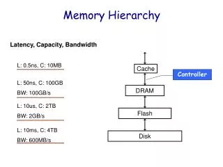
At each level the performance and other features of a particular memory storage type is as below. LEVEL 1:Processor registers – fastest possible access (usually 1 CPU cycle), only hundreds of bytes in size. CPU registers hold words retrieved from cache memory. LEVEL 2: Cache – often accessed in just a few cycles, usually tens of kilobytes.
Cache holds cache lines retrieved from the memory. LEVEL 3: Main memory – may take hundreds of cycles, but can be multiple gigabytes. Access times may not be uniform, in the case of a NUMA machine. Main memory holds disk blocks retrieved from local disks.
LEVEL 4: Flash Memory – faster than disk storage, with up to 4GB or more of data, transferring (usually) over universal serial bus (USB). LEVEL 5: Disk storage – millions of cycles latency, but very large. LEVEL 6: Tertiary storage – tape, optical disk (WORM).
The table summarizes the characteristics of various memory storage:
References: http://en.wikipedia.org/wiki/Memory_hierarchy http://en.wikipedia.org/wiki/Cache_memory http://en.wikipedia.org/wiki/Processor_register http://csapp.cs.cmu.edu/public/ch6-preview.pdf http://homepage.cs.uri.edu/book/cpu_memory/cpu_memory.htm http://www.cs.mun.ca/~paul/cs3725/material/web/notes/node4.html

