Download
1 / 57
600 likes | 949 Vues
High Speed Logic Transmission lines. Transmission lines overview. (1) Characteristics of and applications of Transmission lines (3) Reflections in transmission lines and methods to reduce them Appendix1 Mathematics of transmission lines.

E N D
High Speed Logic Transmission lines Transmission lines (v.3c)
Transmission lines overview • (1) Characteristics of and applications of Transmission lines • (3) Reflections in transmission lines and methods to reduce them • Appendix1 • Mathematics of transmission lines Transmission lines (v.3c)
(1) Characteristics of and applications of Transmission lines • Advantages: • Less distortion, radiation (EMI), cross-talk • Disadvantage • More power required. • Applications, can hanlde • Signals traveling in long distance in Printed-circuit-board PCB • Signals in a cables, connectors (USB, PCI). Transmission lines (v.3c)
Advantage of using transmission lines:Reduce Electromagnetic Interference (EMI) in point-to-point wiring • Wire-wrap connections create EMI. • Transmission lines reduce EMI because, • Current loop area is small, also it constraints the return current (in ground plane) closer to the outgoing signal path, magnetic current cancel each other. Transmission lines (v.3c)
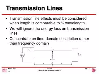
Transmission line problem (Ringing) • Ring as wave transmit from source to load and reflected back and forth. • Solution: Source termination method • or load termination method(see later) Load end Source end Source termination Long transmission line Load termination Transmission lines (v.3c)
The testing board Demo • http://youtu.be/ezGrGXSV3-s Source 32MHz square wave Source Load When R=50 (Matched load) When R=∞ (open circuit) Long transmission line (50 ) Load R=50 Source Transmission lines (v.3c)
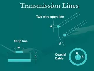
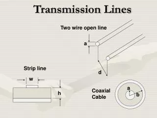
Cross sections of transmission lines to show how constant capacitance and inductance per unit length are maintained Transmission lines (v.3c)
A transmission line Connector and 50 terminator Cross section of Coaxial transmission Transmission lines (v.3c) http://i.ehow.com/images/GlobalPhoto/Articles/5194840/284225-main_Full.jpg
Characteristic of a transmission line • A transmission line has a Characteristic impedance of Z0 • Typically 50 Ohms for a coaxial cable • That means no matter where ( a distance of x meters from the source) you measure the voltage Vx over current Ix at a line is Vx/Ix=50 Ohms Source Zs Load ZL At x, Z0=Vx/Ix=50 Ohms Transmission lines (v.3c)
Reflections in transmission lines Signals inside the line (assume the signal frequency is a constant) Transmission lines (v.3c)
Define voltages/ functions of the line • A=Vi/Vs= Input acceptance function • T= Vt/Vi=Output transmission function • R2 =Vr/Vi=load-end reflective coefficient R2 =Vr/Vi T=Vt/Vi It A=Vi/Vs Ir Ii Rs Vr Vt ZL= Load Vs Z0 R1 Vi Source end Load end Transmission lines (v.3c)
Load-end reflection Load-end reflective coefficient R2 Output transmission function T Transmission lines (v.3c)
R2 T It Ir Ii Z0 Vi Vr Vt Load ZL Find Load-end reflective coefficient R2=Vr/Vi • Vt=Vi+Vr • Vi=Ii Z0 • Ii- Ir =It (kircoff law) • Vi/Z0-Vr/Z0=Vt/ZL • Vi/Z0-Vr/ Z0 =Vi/ ZL +Vr/ZL • Vr/ Z0+Vr/ ZL = Vi/ Z0-Vi/ZL • after rearrangement, hence • R2=Vr/Vi= [ZL- Z0 ]/ [ZL + Z0 ] Transmission lines (v.3c)
(1) Output doubled • R2 in different types of ZL • (case 1)Open circuit at load ZL = • R2=[1-Z0/ ]/[1+Z0/ ]=1 • (*The output is doubled; used in PCI bus) • (case 2) Shorted circuit at load, ZL =0 • R2,= -1 (phase reversal) • (case 3) Matched line ZL = Z0 =characteristic impedance • R2,= 0 (no reflection) (perfect!!) ZL = (2) Signal reflect back To source ZL =0 (3) Perfect Z0 Transmission lines (v.3c)
Load-end transmission Output transmission function T Transmission lines (v.3c)
Derivation for T(): At load-end (Junction between the line and load) R2 T It Ir Ii • Define • Vt=Vi+Vr • Vt/Vi=1+Vr/Vi • and • T= Vt/Vi=Output transmission function =1+Vr/Vi=1+ load-end reflective coefficient (R2) • Hence 1+ R2=T Z0 Vi Vr Vt Load Transmission lines (v.3c)
Output transmission function T=Vt/Vi R2=Vr/Vi T=Vt/Vi It A=Vi/Vs Ir Ii Rs • 1+R2=T=Vt/Vi and • R2=Vr/Vi=[ZL- Z0 ]/[ZL + Z0 ] • Rearranging terms • T=Vt/Vi=1+R2= 2 ZL • [ZL +Z0 ] Vr Vt Load Vs R1 Vi Z0 Transmission lines (v.3c)
Summary of Load-endOutput transmission function T • T=Voltage inside line/voltage at load • T=2 ZL /[ZL +Z0 ] • Also 1+R2=T Characteristic impedance = Z0 Finite length Rs T source ZLZ0 Z0 Transmission lines (v.3c)
Source-end reflection Source-end reflective coefficient R1 Input acceptance function A Transmission lines (v.3c)
Source-end (R1) reflective coefficient • Source end reflective coefficient =R1 • By reversing the situation in the load reflective coefficient case • R1 =[Zs - Z0 ]/[Zs + Z0 ] Characteristic impedance = Z0 Finite length A Rs T source R2 R1 ZLZ0 Transmission lines (v.3c)
Source-endInput acceptance function A • A=Vi/Vs=Voltage transmitted to line/source voltage • A=Z0 /[Zs +Z0 ] , A Voltage divider Characteristic impedance = Z0 Finite length A Zs T R2 source ZLZ0 R1 Transmission lines (v.3c)
Reflections on un-matched transmission lines • Reflection happens in un-terminated transmission line . • Ways to reduce reflections • End termination eliminates the first reflection at load. • Source reflection eliminates second reflection at source. • Very short wire -- 1/6 of the length traveled by the edge (lumped circuit) has little reflection. Transmission lines (v.3c)
A summary • A= Input acceptance func=Z0 /[Zs +Z0 ]. • T=Output transmission func.= 2ZL/[ZL+Z0]=1+ R2 • R2=load-end reflective coef.=[ZL - Z0 ]/ [ZL + Z0 ] • R1=source-end reflective coef.=[Zs - Z0 ]/[Zs + Z0 ] Transmission lines (v.3c)
15 in. Z0=50 9 A T Transmission line 75 1V step R1 R2 A= Input acceptance func. T=Output transmission func. R2=load-end reflective coef. R1=source-end reflective coef. An example • A=Z0 /[Zs+Z0 ]=50/59=0.847 • T=2ZL/[ZL+Z0]=2x75/125=1.2 • R2=[ZL-Z0]/[ZL+Z0)] • = load-end reflective coef.=75-50/125=0.2 • R1=[ZS-Z0 ]/[ZS+Z0] • =Source-end reflective coef.=9-50/59= -0.695 • H=Line transfer characteristic0.94 Transmission lines (v.3c)
Delay=Tp=180ps/in 15in => Tdelay= 2700ps From [1] Transmission lines (v.3c)
Ways to reduce reflections • End termination -- If ZL=Z0, no first reflective would be generated. Easy to implement but sometimes you cannot change the load impedance. • Source termination -- If Zs=Z0 The first reflective wave arriving at the source would not go back to the load again. Easy to implement but sometimes you cannot change the source impedance. • Short (lumped) wire: all reflections merged when • Length << Trise/{6 (LC) } • But sometimes it is not possible to use short wire. Transmission lines (v.3c)
Application to PCI bus from 3.3 to 5.8V • http://direct.xilinx.com/bvdocs/appnotes/xapp311.pdf ZL=un-terminated= T=2ZL/[ZL+Z0 ]=2 So 2.9*2=5.8V Line is short (1.5 inches) so Line transfer characteristic P=1. Vin*A= 3.3*70/(10+70) =2.9V Transmission lines (v.3c)
From: http://direct.xilinx.com/bvdocs/appnotes/xapp311.pdf • [The PCI electrical spec is defined in such a way as to provide open termination incident waveswitching across a wide range of board impedances. It does this by defining minimum andmaximum driving impedances for the ICs output buffers. The PCI specification also stipulatesmandatory use of an input clamp diode to VCC for 3.3V signaling. The reason for this is toensure signal integrity at the input pin by preventing the resultant ringing on low-to-high edgesfrom dipping below the switching threshold. To see this, consider the unclamped case, which isshown in Figure 3. A 3.3V output signal from a 10 ohm source impedance1 into a 70 ohmtransmission line will generate an incident wave voltage of 5.8V at the receiving end. After twoflight delays, a negative reflected wave will follow, getting dangerously close to the upper endof the input threshold2.] Transmission lines (v.3c)
Exercise Input= 1 V step Length L = 10 inches. Characteristic impedance Z0= 75. Source impedance RS= 5. Load impedance RL= 120. Line transfer characteristic P = 0.9. Time delay per inch of the line Tp= 160 ps/in. • Sketch the waveform of the signal at the load between the time is 0 and the time when the signal is reflected back to the load end the second time. Mark clearly the time and voltage levels when the signal reaches the load the first time and the second time. • How do you change the values of RL and RS if you want to have a 0.5 V voltage step at the output without ripples? • What is the highest output voltage for all possible RL and RS? • How do you change the values of RL and RS if you want to have a peak of 1.3 V voltage at the output (ripples are allowed)? • Describe with explanation two methods to reduce reflections in a transmission line. Transmission lines (v.3c)
answer • Similar to the example discussed. • How do you change the values of RL and RS if you want to have a 0.5 V voltage step at the output without ripples? (answer: two methods (i) set Rs=Z0 for no source reflection, RL=93.75 Ohms. (ii) set RL=75 Ohms , no load reflection, Rs =60 Ohms) • What is the highest output voltage for all possible RL and RS? ANS:(RS=0, RL=infinity) Vout=p*Tmax=0.9*2V • How do you change the values of RL and RS if you want to have a peak of 1.3 V voltage at the output (ripples are allowed)? ANS: p*T=0.9*2*RL/(Z0+RL)=1.3, (Rs=0, RL=195). You may use a small value for RS similar to the PCI bus, say 10 . Transmission lines (v.3c)
Conclusion • Studied Characteristics of transmission lines. • Studied ways to terminate the line to avoid reflection. Transmission lines (v.3c)
References • [1]Chapter4 of High speed digital design , by Johnson and Graham • [2] Kreyszig, Advanced Engineering maths, edition 6, Page 74 • [3] Buckley, Transmissions networks and circuits , The Macmillan press. Page 1 • [4]http://direct.xilinx.com/bvdocs/appnotes/xapp311.pdf (For PCI application) Transmission lines (v.3c)
Appendix 1 Transmission lines (v.3c)
Mathematics of transmission lines Transmission lines (v.3c)
Main formulas (for proof, see appendix 1) • If = [(R+ j L)(G+j C)] • V=Ae-x +Bex ----------------------(13) • I=(A/Z0)e-x - (B/Z0)ex ------------(14) • Z0= [(R+j L)/(G+j C)]=characteristic impedance Transmission lines (v.3c)
Incident and reflective waves Source termination Long transmission line (characteristic impedance Zo, typically = 50 Ohms) Load termination • Vx=Ae-x +Bex • Ix=(A/Z0)e-x -(B/Z0)ex • = [(R+ j L)(G+j C)] • Z0= [(R+j L)/(G+j C)]=characteristic impedance x Vx=voltage at X Ix=current at X Reflective wave Incident wave Transmission lines (v.3c)
Characteristics of ideal Transmission lines • Ideal lossless transmission lines • infinite in extent • signals on line not distorted/ attenuated • but it will delay the signal measured as picoseconds/inch, this delay depends on C and L per unit length of the line. (by EM wave theory) • Delay (ps/in)=10+12 [(L per in)*(C per in)] • Characteristic impedance = [L per in/C per in] Transmission lines (v.3c)
Appendix 1 Math of transmission lines Transmission lines (v.3c)
Characteristics of ideal Transmission lines • Ideal lossless transmission lines • infinite in extent • signals on line not distorted/ attenuated • but it will delay the signal measured as picoseconds/inch, this delay depends on C and L per unit length of the line. (by EM wave theory) • Delay (ps/in)=10+12 [(L per in)*(C per in)] • Characteristic impedance = [L per in/C per in] Transmission lines (v.3c)
Step response of transmission lines (by EM wave theory) Transmission lines (v.3c)
Delay and impedance of ideal transmission lines • Step (V) input to an ideal trans. line (X to Y) with C per in =2.6pF/in, L per in =6.4nH/in . • Cxy=(C per in)(Y-X) • Charge held (Q)= Cxy V=(C per in)(Y-X)V • Per unit length Time delay (T)=(Y-X) [(L per in)(C per in)] • Current=I=Q/T • I= (C per in)(Y-X)V = V* (C/L) • {(Y-X){[(L per in)(C per in)]}1/2 • Z0=V/I= (L per in /C per in )=(6.4 nH/2.6 pF) 1/2 =50 By EM wave theory Transmission lines (v.3c)
A quick reference of the important transmission line formulas • V= Ae-x + Be +x • I = (A/Z0)e-x - (B/Z0)e +x • Where A, B are constants. • Z0 =characteristic impedance is real. • = propagation coefficient is complex Derivations will be shown later Transmission lines (v.3c)
A small segment For a small segment x A long transmission line • R=resistance; G=conductance; C=capacitance; L=inductance. All unit length values. v R x L x i v C x G x x Transmission lines (v.3c)
For the small segment of wire • --(horizontal voltage loop) • -(v/ x) x=R x i + L x ( i/ t) • --(vertical current loop) • -(i/ x) x=G x v + C x ( v/ t) • -(v/ x)=Ri+L( i/ t) ------------------(1) • -(i/ x)=Gv+C( v/ t) ------------------(2) • Applying phasor equations, I,V depend on x only , not t • v=Vej t --------------------------------------(3) • i=Iej t ----------------------------------------(4) Transmission lines (v.3c)
Applying phasor equations, I,V depend on x only, not tBut v,i depend on t and xv = Vej t ---------------------------------------(3)i = Iej t ----------------------------------------(4) • Hence from (3) and (4) • (v/ x)= ej t(dV / d x) --------------------(5) (v/ t)= j V ej t--------------------------(6) • (i/ x)= ej t(d I / d x) ----------------------(7) • (i/ t)= j I ej t----------------------------(8) Since in general, ekt / t = k ekt Transmission lines (v.3c)
Put 5,4,8 into 1 • -(v/ x)=Ri+L( i/ t) -------------(from 1) • -(dV /d x )ej t = R I ej t + L j I ej t • -(dV /d x )= (R+j L)I --------------------(9) • => -(d2V/dx2)=(R+j L)dI/dx • = -(R+j L)(G+j C)V • (d2V/dx2) = +2V --------------------------(11) • where = [(R+ j L)(G+j C)] (8) (5) (4) (10, see next page) Transmission lines (v.3c)
Put 7,3,6 into 2 • -(i/ x)=Gv+C( v/ t) ------------(from 2) • -(dI /d x )ej t = G V ej t + Cj V ej t • -(dI /d x )= (G+j C)V-----------------(10) • => -(d2I/dx2)=(G+j C)dv/dx • = -(G+j C)(R+j L)I • (d2I/dx2) = + 2I --------------------------(12) • where = [(R+ j L)(G+j C)] (6) (7) (3) (9, see previous page) Transmission lines (v.3c)
From the wave equation form(see [2] , Homogeneous 2nd order differential equations, also see appendix2,3) • (d2V/dx2) = 2V -------(11) • (d2I/dx2) = 2I ---------(12) • where = [(R+ j L)(G+j C)] • Solution is • V=Ae-x +Bex ----------------------(13) • Differentiate (13) and put into (9), see appendix 2 • I=(A/Z0)e-x - (B/Z0)ex ------------(14) • Z0= [(R+j L)/(G+j C)]=characteristic impedance Transmission lines (v.3c)
Different transmission lines • (Case 1) Infinite transmission line; impedance looking from source is the characteristic impedance Z0. • (Case2) Matched line (finite line with load connected to Z0) has the same property as an infinite transmission line • (Case3) unmatched line : reflection will occur Transmission lines (v.3c)
(Case1) Infinite transmission line • For Infinite line, the impedance is the characteristic impedance Z0 Characteristic impedance = Z0 Impedance looking from source= Z0 Transmission lines (v.3c)