Differencing Multistage Detector
ELEC422 Course Project. Differencing Multistage Detector. Gang Xu, Praful Kaul, Sridhar Rajagopal Electrical and Computer Engineering Department, Rice University, Houston,TX. Background and Algorithm. Multiuser detector architecture for next generation CDMA base station

Differencing Multistage Detector
E N D
Presentation Transcript
ELEC422 Course Project Differencing Multistage Detector Gang Xu, Praful Kaul, Sridhar Rajagopal Electrical and Computer Engineering Department, Rice University, Houston,TX.
Background and Algorithm • Multiuser detector architecture for next generation CDMA base station • Advanced Interference cancellation • Computation efficient algorithm
Description of the Chip -- MUDDY • 8 synchronous mobile users • 12-bit fixed point arithmetic • 10-bit input/output interface • 6100 transistors • 34 pins • Cascade of 3 chips
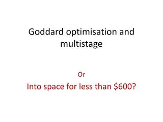
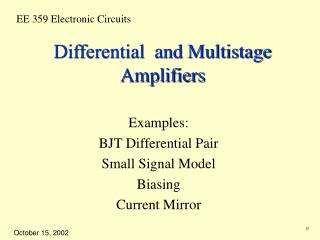
DEMUX A L U << ENCODER Block Diagram
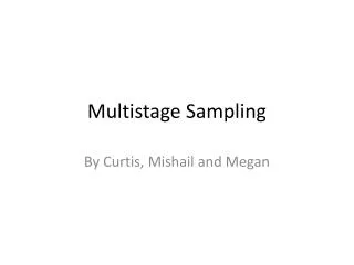
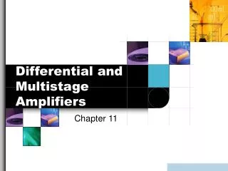
FOUT O0 O1 O2 O3 GND O4 O5 O6 O7 Vdd O8 O9 GND HO 1#/2 40 39 38 37 36 35 34 33 32 31 30 29 28 27 26 25 24 23 22 21 M U D D Y 1 2 3 4 5 6 7 8 9 10 11 12 13 14 15 16 17 18 19 20 I0 I1 I2 I3 I4 Vdd I5 I6 I7 GND I8 I9 Prev HI Vdd ClkB ClkA LD FIN/RST I0-I9 Soft Decision/ Cross-correlationInput PREV HI - Previous Hard Decision Input O0- O9 Soft Decision Output HO - Hard Decision Input Pin Description LOAD - Load cross-correlation matrix FIN/RST - Finish input/Reset FOUT - Finish Output 1#/2 - First/Second (Third) Chip
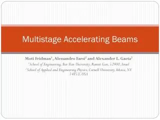
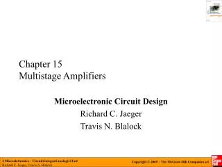
0/11 0/10 0 10/701 1 10/001 7 0 01/710 01/010 0/10 0/10 1 7 Reset 10/601 10/101 01/110 2 6 01/610 Reset 2 6 0/10 0/10 01/510 01/210 3 10/501 10/201 5 PLA III 0/10 3 4 0/10 5 Main PLA 01/310 01/410 Load/reset WB Change ABS/addr finish RD2 WR2 10/401 10/301 4 0/00000 0 11 01/0001 1 0 01/7010 0/00011 0/00000 1 10/0110 8 01/7001 01/1001 Reset 10/7010 2 10 10/1010 Reset 7 0/00001 2 0/00000 01/6001 PLA II 10/6010 10/2010 01/2001 3 9 6 PLA I 3 10/5010 0/00001 0/00001 10/3010 Load WB /addr WR1 WR3 01/5001 10/4010 Reset/RD1 change 5 01/3001 4 4 8 0/00001 0/00001 5 7 0/00001 6 0/00001 State Diagram
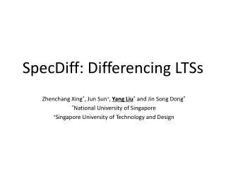
Standard Cells 3-8 Decoder Shift Register Cell Register Cell 3-bit Comparator 2-1 MUX
Critical Path Analysis ALU is the critical path IRSIM Simulation 25ns Crystal Simulation : 42.63ns Spice Simulation 20ns. Max. Clock Frequency 25 MHz*