Semiconductor Diode
Semiconductor Diode. Instructor: Farzana Rahmat Zaki Senior Lecturer, EEE Eastern University. Lecture-7. Diode rectifier circuit Half wave rectifier Full wave rectifier Peak rectifier. Rectifier Circuits. A rectifier is an electrical device that converts an AC signal to DC signal.


Semiconductor Diode
E N D
Presentation Transcript
Semiconductor Diode Instructor: Farzana Rahmat Zaki SeniorLecturer, EEE Eastern University CSE 177/ EEE 177
Lecture-7 Diode rectifier circuit Half wave rectifier Full wave rectifier Peak rectifier CSE 177/ EEE 177
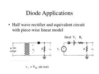
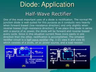
Rectifier Circuits CSE 177/ EEE 177 A rectifier is an electrical device that converts an AC signal to DC signal. Rectifiers are used as components of power supplies and as detectors of radio signals. Rectifiers may be made of diode components. There are two types of rectifier circuits: (a) Half-wave rectifier and (b) Full-wave rectifier. 3
Half Wave Rectifier V0 = 0, vs< VD0 V0 = (vs – VD0)× R / (R + rD), vs ≥VD0 as, rD << R, so V0 ≈ (vs – VD0) for vs ≥ VD0 Transfer characteristic curve CSE 177/ EEE 177 Utilizes alternate half-cycles of input sinusoid. Diode is modeled using piecewise linear model. 4
Half Wave Rectifier (contd.) • In selecting diodes for rectifier design, 2 parameters must be specified : • Current handling capability required of the diode, (determined by the largest current the diode is expected to conduct.) (b) PIV (peak inverse voltage) that the diode must be able to withstand without breakdown, (determined by maximum reverse bias voltage appearing across the diode.) For half wave rectifier, PIV = VS * It is usually prudent, however to select a diode that has a reverse breakdown voltage at least 50% greater than the expected PIV. CSE 177/ EEE 177
Full Wave Rectifier CSE 177/ EEE 177 • Full wave rectifier utilizes both halves of the input sinusoid. • To provide a uni-polar output, it converts the negative halves of the sine wave. • Full wave rectification can be obtained in two ways- - Full wave rectifier using a transformer with a center-tapped secondary winding - Full wave Bridge Rectifier 6
Full Wave Rectifier utilizing a transformer with a center-tapped secondary winding CSE 177/ EEE 177 • Secondary XFR winding is center-tapped to provide two equal voltages (vs) across the two halves of secondary windings • During +ve half cycle, D1 -------- On D2 --------- Off • Current (I) will flow through D1, R and Back to sec. center tap coils. Output voltage, V0 = vs – VD 7
CSE 177/ EEE 177 • During -ve half cycle, D2 ---------- On D1 ---------- Off • Current (I) will flow through D2 , R & will back to sec. tap Winding. Output voltage, V0 = vs – VD 8
During positive half cycle, D1 is ON & D2 is OFF. Voltage at cathode of D2 = v0 & anode = -vs So, reverse voltage across D2 = v0 + vs It will reach its maximum value, when v0 = VS – VD vs = VS So, PIV = 2VS - VD PIV calculation for full-wave rectifier (center tapped) CSE 177/ EEE 177
The Bridge Full wave Rectifier CSE 177/ EEE 177 The circuit is known as bridge rectifier because of the similarity of its configuration to that of Wheatstone bridge. No center-tapped transformer is required Bridge rectifier is inexpensive as one can buy a bridge rectifier in one package.
Operation of Bridge Rectifier CSE 177/ EEE 177 • During +ve half cycle, D1 and D2 are ON D3 and D4 are Off. • Current (I) will flow through D1,R, D2 and back to XFR. • O/p voltage,V0= vs- 2VD
CSE 177/ EEE 177 • During -ve half cycle, D1 and D2 are Off D3 and D4 are On. • Current (I) will flow through D3,R, D4 and back to XFR. • O/p voltage,V0= vs- 2VD
PIV of each diode: Let determine reverse voltage across D3 during positive half cycle of input. Consider loop formed by D3, R,D2. vD3(reverse)= v0 + vD2(forward) so, PIV = VS – 2VD + VD = VS – VD PIV calculation for Bridge rectifier CSE 177/ EEE 177
Advantages of bridge rectifier • ½ the PIV of the full wave • Don’t need a center-tapped transformer • Only need half of the turns in the secondary winding CSE 177/ EEE 177
Filter capacitor • The pulsating nature of the output voltage produced by the rectifier circuits, makes it unsuitable as a dc supply for electronic circuits. • A simple way to reduce the variation of the output voltage is to place a capacitor across the load resistor. This capacitor is known as Filter Capacitor. • Filter capacitor serves to reduce substantially the variations in the rectifier output voltage. CSE 177/ EEE 177
Operating principle: v1 be a sinusoid input with a peak value of VP and assume the diode to be ideal. As v1 goes positive, diode conducts & capacitor is charged so that v0 = v1. This situation continues until v1 reaches to VP. Beyond the peak, as v1 decreases, diode goes to reverse biased and v0 remains same (constant) as there is no path for capacitor to discharge. Thus the circuit provides a dc voltage output equal to the peak of input sine wave. Effect of Filter Capacitor CSE 177/ EEE 177
Assume, diode to be ideal. For an sine input, the capacitor charges to the peak of the input, Vp. Then, diode operates in cut off mode and capacitor discharges through the load R. The capacitor discharge will continue for almost the entire cycle, until v1 exceeds the capacitor voltage. Then the diode turns on again, charges the capacitor up to peak of v1 and the process repeats itself. In order to keep the output voltage from too much decreasing during capacitor discharge, one should select a value for C so that time constant, RC >> discharging interval. The rectifier with a filter capacitor- Peak Rectifier CSE 177/ EEE 177
During the diode-off interval, v0 = VP e-t/RC At the end of discharge interval, VP – Vr = VP e-T/RC As RC>>T, e-t/RC = 1 – T/RC VP – Vr = VP (1 – T/RC) So, Vr = VpT/RC = Vp/ (f×C×R) Conduction angle, ωΔt = √(2×Vr /Vp) Average diode current, iDAV= IL{1+π√(2×Vp/Vr)} Maximum diode current, iDMAX= IL{1+2π√(2×Vp/Vr)} Expression for ripple voltage (Vr), conduction angle, iD (avg. and max.) CSE 177/ EEE 177
Example-3.10 • Consider a peak rectifier fed by 60Hz sinusoid having a peak value Vp=100V. Let the load resistance R = 10kΏ. Find the value of the capacitance C that will result in a peak ripple of 2V. Also calculate the fraction of the cycle during which the diode is conducting, the average and peak values of the diode current. Solution: C = Vp / (VrfR) = 83.3μF Conduction angle, ωΔt = √(2×Vr /Vp) = 0.2 rad IL = 100/10 = 10mA Average diode current, iDAV= IL{1+π√(2×Vp/Vr)} = 324mA Maximum diode current, iDMAX= IL{1+2π√(2×Vp/Vr)}=638mA CSE 177/ EEE 177
Uses of Peak rectifier circuit • Used in signal processing systems where it is required to detect the peak of an input signal. In such a case, the circuit is referred to as a peak detector. • Peak detector is used in the design of a demodulator for amplitude modulated (AM) signal. CSE 177/ EEE 177