ECE260B – CSE241A Winter 2005 Parasitic Extraction
710 likes | 1k Vues
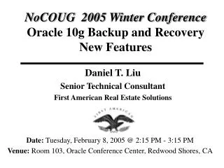
ECE260B – CSE241A Winter 2005 Parasitic Extraction. Website: http://vlsicad.ucsd.edu/courses/ece260b-w05. Funct. Spec. RTL. Behav. Simul. Stat. Wire Model. Logic Synth. Gate-level Net. Front-end. Gate-Lev. Sim. Floorplanning. Back-end. Parasitic Extrac. Place & Route. Layout.

ECE260B – CSE241A Winter 2005 Parasitic Extraction
E N D
Presentation Transcript
ECE260B – CSE241AWinter 2005Parasitic Extraction Website: http://vlsicad.ucsd.edu/courses/ece260b-w05
Funct. Spec RTL Behav. Simul. Stat. Wire Model Logic Synth. Gate-level Net. Front-end Gate-Lev. Sim. Floorplanning Back-end Parasitic Extrac. Place & Route Layout Conventional Design Flow
Technology Scaling • Process technology evolves with shrinking feature sizes • Parasitic effects become more significant with smaller feature sizes • Increasing wire resistance, fringing and coupling capacitances... • Interconnect delay dominates VLSI system performance • The performance of today’s DSM ICs is strongly determined by the parasitic effects of the passive structures interconnecting active devices • Accurate, high-speed tools and methods are needed to extract and simulate these parasitic effects in order to perform precise timing analysis to the circuit
Layout Parasitic Extraction • Necessary step after routing • Back-annotation • Account for non-ideal nature of interconnect • Wire capacitance • Wire and via resistance • Parasitic information is used in post-layout verification • Timing verification of synchronous circuits • Functional verification of asynchronous circuits • Design performance is ultimately limited by parasitics
R4 R2 C2 C4 Ri Ci Parasitic Extraction: Why do we need it? 2 • Example: to produce RC tree network for elmore delay analysis • Example: to produce RC tree network for capacitive cross-talk analysis R1 4 1 s R3 C1 3 C3 i Slide courtesy L. Daniel
Parasitic Extraction thousands of wires e.g. critical path e.g. gnd/vdd grid Parasitic Extraction • identify some ports • produce equivalent circuit that models response of wires at those ports tens of circuit elements for gate level spice simulation Slide courtesy L. Daniel
Electromagnetic Analysis small surface panels with constant charge thin volume filaments with constant current million of elements Model Order Reduction tens of elements Parasitic Extraction (the two steps) Slide courtesy L. Daniel
Parasitic Extraction / Back-Annotation • Input data • Technology data • Metal and via resistances • Capacitance coefficients • Library data • Input pin capacitances • Design data • Routing • Boundary conditions (load and drive information) • Output data • Parasitic information: • DSPF • RSPF • Set_load • Interpreted parasitic information • Custom WLM • LEF coefficients
Active Device Parasitics • Gate output capacitance mainly from gate oxide tox • Substrate coupling resistances and capacitances • Characterized by cell libraries Figure courtesy, A. Nardi
Interconnect Parasitics • Wires are not ideal. Parasitics: • Resistance • Capacitance • Inductance • Why do we care? • Impact on delay • noise • energy consumption • power distribution Picture from “Digital Integrated Circuits”, Rabaey, Chandrakasan, Nikolic Slide courtesy L. Daniel
Passivation Dielectric Wire Etch Stop Layer Via Global (up to 5) Dielectric Capping Layer Copper Conductor with Barrier/Nucleation Layer Intermediate (up to 4) Local (2) Pre Metal Dielectric Tungsten Contact Plug SEMATECH Prototype BEOL stack, 2000 • Slide courtesy of Chris Case, BOC Edwards
Interconnect Resistance L r R = T W Sheet Resistance L R T R R 1 2 W • Resistance seen by current going from left to right is same in each block
Resistance Scaling • Resistance scales badly • True scaling would reduce width and thickness by S each node • R ~ S2 for a fixed line length and material • Reverse scaling wires get smaller and slower, devices get smaller and faster • At higher frequencies, current crowds to edges of conductor (thickness of conduction = skin depth) increased R
Interconnect Capacitance Lateral cap w S • Line dimensions: W, S, T, H • Sometimes H is called T in the literature, which can be confusing
Capacitance Estimation • Empirical capacitance models are easiest and fastest • Handle limited configurations (e.g., range of T/H ratio) • Some limiting assumptions (e.g., no neighboring wires) • Rules of thumb: e.g., 0.2 fF/um for most wire widths < 2um • Cf. MOSFET gate capacitance ~ 1 fF/um width • Pattern-matching approaches applied to multilayer cross-sections Capacitance per unit length
d d Self Inductance d d Mutual Inductance Inductance • Inductance is the flux induced by current variation • Measures ability to store energy in the form of a magnetic field • Consists of self-inductance and mutual inductance terms • At high frequencies, can be significant portion of total impedance Z = R + jwL (w = 2pf = angular freq)
Coil Inductance • V = L d I/d t V2 = M12 d I1/d t • Faraday’s law V = N d (B A) / d t B = m (N / l) I L = m N2 A / l V = voltage N = number of turns of the coil B = magnetic flux A = area of magnetic field circled by the coil l = height of the coil t = time
Filament Inductance Where the integral is over the volume of the conductors, • r is the position in a given filament, and • li is the unit vector in the direction of current flow for conductor i
Inductance Scaling • If where • Copper interconnects R is reduced • Faster clock speeds • Thick, low-resistance (reverse-scaled) global lines • Chips are getting larger long lines large current loops • Frequency of interest is determined by signal rise time, not clock frequency Massoud/Sylvester/Kawa, Synopsys • Slide courtesy of Massoud/Sylvester/Kawa, Synopsys
Inductance Trends • Inductance = weak (log) function of conductor dimensions • Inductance = strong function of distance to current return path (e.g., power grid) • Want nearby ground line to provide a small current loop (cf. Alpha 21164) • Inductance most significant in long, low-R, fast-switching nets • Clocks are most susceptible
Inductance is Important … • On-chip inductance is negligible, and usually alleviate performance degradation due to the presence of capacitance • Seesaw effect between inductance and capacitance • Package inductance is significant when coupled with large magnitude of currents in the same frequency range • Complete analysis needs to include package inductance since signals cannot be assumed ideal at pads • For the idealized case of a lossless homogeneous dielectric with an array of conductors, the inductance matrix [L] can be derived directly from the capacitance matrix [C] by where v0 is the phase velocity of the medium • However in the IC domain, these assumptions do not hold up and we need inductance extraction
Inductance Return Path • Inductance is a loop quantity • Knowledge of return path is required, but hard to determine • For example, the return path depends on the frequency Signal Line Return Path Massoud/Sylvester/Kawa, Synopsys • Slide courtesy of Massoud/Sylvester/Kawa, Synopsys
Signal Gnd Gnd Gnd Gnd Gnd Gnd Signal Gnd Gnd Gnd Gnd Gnd Gnd Frequency-Dependent Return Path • At low frequency, and current tries to • minimize impedance • minimize resistance • use as many returns as possible (parallel resistances) • At high frequency, and current tries to • minimize impedance • minimize inductance • use smallest possible loop (closest return path) L dominates, current returns “collapse” • Power and ground lines always available as low-impedance current returns • Slide courtesy of Massoud/Sylvester/Kawa, Synopsys
Extracting Inductance vs. Capacitance • Capacitance • Locality problem is easy: electric field lines “suck up” to nearest neighbor conductors • Boundary element approach requires discretization of only the surfaces of conductors • Charge density over the conductor is rarely uniform, needs to solve the integral form of Laplace’s equation for many times • Inductance • Locality problem is hard: magnetic field lines are not local; current returns can be complex • Local calculation is easy: no strong geometry dependence; analytic formulae work very well • Current density and direction is constant in each conductor when the frequency is low enough to ignore the skin effect • Conductors are divided into bundles of filaments each with a constant current density, compute a circuit solution for return current distribution
Outline • Problem Statement • Parasitics • Extraction Methods • Resistance extraction • Capacitance Extraction (electrostatic) • RL Extraction (MQS) • Combined RLC Extraction (EMQS) • Electromagnetic Interference Analysis (fullwave) • Future Trends
Interconnect Resistance Extraction • Sheet resistance R□ • Series resistance R = R□ * Length / Width / Thickness • Inaccuracies arise in irregular geometries, e.g., corners of a route • Apply Laplace’s equation 2=0, or • Discretize an interconnect conductor into grids • Solve a partial differential equation with known boundary conditions • Table Lookup for better efficiency
Outline • Problem Statement • Parasitics • Extraction Methods • Resistance extraction • Capacitance Extraction (electrostatic) • RL Extraction (MQS) • Combined RLC Extraction (EMQS) • Electromagnetic Interference Analysis (fullwave) • Future Trends
Parasitic Extraction Accuracy • Above 0.5μm feature size, wire cross-section was rectangular • Interconnect modeled as parallel plate over ground plane • Parallel plate capacitance • Fringe capacitance • 2-D extraction accurate enough: Area + Fringe C_parallel C_fringe C_fringe
Capacitance Extraction • 2-D extraction • Wire cap includes parallel plate (area), fringing, and coupling cap • C = k1 Area + k2 Perimeter + k3 Coupling_length / Coupling_spacing • These coefficients are fit in for an average environment of a wire • Table Lookup • Intra-layer capacitances are not well modeled • 3-D extraction • Solve for real 3-D geometries of wiring • 2.5-D extraction • Compromise between speed and accuracy • Models 3-D effects by a combination of two orthogonal 2-D structures • E.g., two cross-section views on the x-z and y-z planes, z is the vertical axis going through layers
How Capacitance Extractor Works • Technology pre-characterization • generates coefficients through solving the 3-D equations for “representative” sample of topologies • Really, cross-sections through “tunnel” that contains a section of the victim net • Creates look-up table • Time consuming, but only done once • Each layer of interconnect added roughly doubles time for coefficient generation • Pattern compression • Reduces the total number of pre-characterization patterns • Geometric parameter extraction • Reduce the number of geometric parameters considering the shielding effect • Extraction matches topologies to entries in look-up table
Extraction to Floating Metal • Dummy fills (as floating metals) are required by modern CMP process • Extraction to floating metal similar to extraction for cross talk analysis • Net to net capacitance required • Effective capacitance to floating metal dependent on potential of floating metal • E.g., Cadence HyperExtract models floating metal as grounded • If we model floating metal as grounded, this is pessimistic • Below 0.18m with “local fill” requirements, fill metal can impact timing Floating metal
Consider only electric field (capacitive) coupling Capacitive ExtractionExample: Intel 0.25 micron Process 5 metal layers Ti/Al - Cu/Ti/TiN Polysilicon dielectric. Taken from “Digital Integrated Circuits”, 2nd Edition, Rabaey, Chandrakasan, Nikolic Slide courtesy L. Daniel
Capacitive ExtractionWhy? E.g. Analysis of Delay of Critical Path
Capacitance ExtractionProblem Formulation • Given a collection of N conductors (of any shape and dimension) Calculate the coupling capacitance matrix C Slide courtesy L. Daniel
Capacitance ExtractionSolution Procedure • For i = 1 to N, • apply one volt to conductor i and ground all the others • solve the electrostatic problem and find the resulting vector of charges on all conductors • that is the i-th column of the conductance matrix Slide courtesy L. Daniel
Overview • Problem Statement • Parasitics • Extraction Methods • Capacitance Extraction (electrostatic) • RL Extraction (MQS) • Combined RLC Extraction (EMQS) • Electromagnetic Interference Analysis (fullwave) • Future Trends
Inductance and Resistance ExtractionExample: IC package Picture Thanks to Coventor wire bonding lead frames IC package Slide courtesy L. Daniel
Inductance and Resistance ExtractionWhere do we need to account for inductance? • chip to package and package to board connections are highly inductive • inductance can create Ldi/dt noise on the gnd/vdd network • inductance can limit communication bandwidth • inductive coupling between leads or pins can introduce noise pins or solder balls from package to PCB wire bonding and lead frames or solder balls from IC to package IC package PCB on-package decoupling capacitors on-board decoupling capacitors Slide courtesy L. Daniel
Simple Example Inductance and Resistance Extraction Why also resistance? Skin and Proximity effects proximity effect: opposite currents in nearby conductors attract each other skin effect: high frequency currents crowd toward the surface of conductors Slide courtesy L. Daniel
Inductance and Resistance ExtractionSkin and Proximity effects (cont.) • Why do we care? • Skin and proximity effects change interconnect resistance and inductance • hence they affect performance (propagation delay) • and noise (magnetic coupling) • When do we care? • frequency is high enough that wire width OR thickness are less than two “skin-depths” • e.g. on PCB at and above 100MHz • e.g. on packages at above 1GHz • e.g. on-chip at and above 10GHz • note. clock at 3GHz has significant harmonics at 10GHz!! Slide courtesy L. Daniel
Inductance and Resistance ExtractionProblem Formulation • Given a collection of interconnected N wires of any shape and dimension • Identify the M input ports Picture by M. Chou • Calculate the MxM resistance and the inductance matrices for the ports, • that is the real and immaginary part of the impedance matrix Slide courtesy L. Daniel
Inductance and Resistance ExtractionSolution Procedure • Typically instead of calculating impendance we calculate the admittance matrix. • For each pair of input terminals, • apply a unit voltage source and solve magneto quasit-static problem(MQS) to calculate all terminal currents • that is one column of the admittance matrix [R+jwL]-1 Slide courtesy L. Daniel
Overview • Problem Statement • Parasitics • Extraction Methods • Capacitance Extraction (electrostatic) • RL Extraction (MQS) • Combined RLC Extraction (EMQS) • Electromagnetic Interference Analysis (fullwave) • Future Trends Slide courtesy L. Daniel
Combined RLC ExtractionExample: current distributions on powergrid input terminals Slide courtesy L. Daniel
Combined RLC Extraction Example: analysis of resonances on powergrid * 3 proximity templates per cross-section - 20 non-uniform thin filaments per cross-section Slide courtesy L. Daniel
Combined RLC ExtractionExtraction Example: analysis of substrate coupling Slide courtesy L. Daniel
Combined RLC ExtractionExample: resonance of RF microinductors • At frequency of operation the current flows in the spiral and creates magnetic energy storage (it works as an inductor: GOOD) • But for higher frequencies the impedance of the parasitic capacitors is lower and current prefers to “jump” from wire to wire as displacement currents (it works as a capacitor: BAD) Picture thanks to Univ. of Pisa Slide courtesy L. Daniel
Combined RLC ExtractionProblem Formulation • Given a collection of interconnected N wires of any shape and dimension • Identify the M input ports Picture by M. Chou • Calculate the MxM IMPEDANCE matrix for the ports, • that is the real and immaginary part of the impedance matrix Slide courtesy L. Daniel
Combined RLC ExtractionSolution Procedure • Same as RL extraction. • Typically calculate admittance matrix • For each pair of input terminals, • apply a unit voltage source and solve electro-magneto quasit-static problem (EMQS) to calculate all terminal currents • that is one column of the admittance matrix [R+jwL]-1 Slide courtesy L. Daniel
Outline • Problem Statement • Parasitics • Extraction Methods • Capacitance Extraction (electrostatic) • RL Extraction (MQS) • Combined RLC Extraction (EMQS) • Electromagnetic Interference Analysis (fullwave) • Future Trends Slide courtesy L. Daniel