Download
1 / 9
90 likes | 183 Vues
Learn how a ground plane reduces loop area, minimizes inductance, and improves signal integrity in printed circuit board layouts. Discover the advantages of using a ground plane for return-current paths in electronics design.

E N D
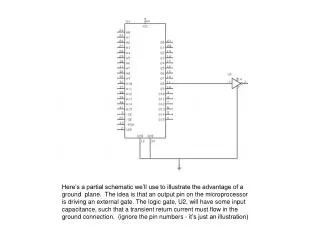
Here’s a partial schematic we’ll use to illustrate the advantage of a ground plane. The idea is that an output pin on the microprocessor is driving an external gate. The logic gate, U2, will have some input capacitance, such that a transient return current must flow in the ground connection. (ignore the pin numbers - it’s just an illustration)
This layout provides a return-current path with a large loop area. Inductance is a complicated function of geometry, but in general it increases with increasing loop area.
Our schematic effectively looks like this. A step change in voltage on the processor pin will resulting in ringing of the parasitic LC circuit, possibly resulting in unintended transisitions of the inverter output.
Using a ground plane on the back side (solder side) of the board reduces the loop area. But why? Where will the return current flow? .
If the return current takes the shortest path - the path of least resistance – the loop area is roughly the same as before.
But the transient current will take the path of least impedance, which is to say, least inductance, and therefore the one with the minimum loop area. The ground plane provides a return path directly underneath the trace, no matter how the trace is routed.
Now let’s suppose we need to route a signal which must cross the previous signal. The crossover trace on the back side only removes a small amount of copper, but completely disrupts the return current path. If crossovers like this can’t be avoided, then it’s time to go to a 4-layer board where an entire inner layer can be committed to the ground plane.
4-layer PCBs from ExpressPCB 1.75 mils, 1.25oz Cu 12 mils, k=4.6 1.4 mils, 1oz Cu 28 mils, k=4.7 1.4 mils, 1oz Cu 12mils, k=4.6 1.75 mils, 1.25oz Cu (Via to inner layer)