Download
1 / 27
280 likes | 496 Vues
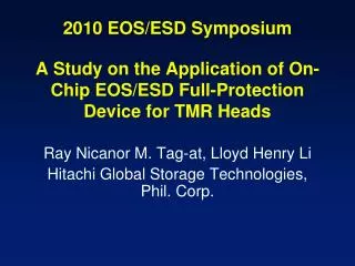
A Study on the Application of On-Chip EOS/ESD Full-Protection Device for TMR Heads. Ray Nicanor M. Tag-at, Lloyd Henry Li Hitachi Global Storage Technologies, Phil. Corp. Objectives. To study and understand the different ESD protection devices for TMR Heads.

E N D
A Study on the Application of On-Chip EOS/ESD Full-Protection Device for TMR Heads Ray Nicanor M. Tag-at, Lloyd Henry Li Hitachi Global Storage Technologies, Phil. Corp.
Objectives • To study and understand the different ESD protection devices for TMR Heads. • To have an effective ESD protection devices that could enhance the robustness of the TMR heads.
Outline • Introduction • Experimental Setup • Results • I-V and R-V Characteristic Curves • Shunt Diode’s Behavior • Charging Mechanism of Diodes • On-chip Diode Shunting Concept • Conclusions
Outline • Introduction • Experimental Setup • Results • I-V and R-V Characteristic Curves • Shunt Diode’s Behavior • Charging Mechanism of Diodes • On-chip Diode Shunting Concept • Conclusions Slide 4
Introduction • Shunting is a commonly used method for on-chip ESD protection. • Diode can also work as a shunt across the TMR sensor. • Commonly installed across tester’s TMR input terminals. • Protects from electrical transients and EOS. • There are already many published studies about diode shunting in GMR/TMR heads. Slide 5
Introduction What are the downsides of this method? • Diodes can also be charged up through its capacitance. • TMR heads has no protection on the rest of the assembly process. Is it then possible to install shunt diodes into the device itself? Slide 6
Outline • Introduction • Experimental Setup • Results • I-V and R-V Characteristic Curves • Shunt Diode’s Behavior • Charging Mechanism of Diodes • On-chip Diode Shunting Concept • Conclusions Slide 7
Experimental Set-up • PSPICE Simulation • Head Gimbal Assembly (HGA) Testers • Quasi Static Tester (QST) • Dynamic Electrical Tester (DET) • Current Transients: Tek CT-6 • Input Signal Measurement: Tek P6248 Diff. Probe • Diode: metal-to-silicon junction Schottky diode D1N5711, Vth=0.3V • HGAs Slide 8
Diode’s Characteristic p- doped n-doped • P-N semiconductor diode has insulating region so-called the “depletion region.” Depletion Region • Depletion Region dictates the flow of current. • It becomes conductive in Forward Bias and remains insulative at Reverse Bias. Diode’s capability to become conductive means that it can be used as shunting device. Slide 9
Outline • Introduction • Experimental Setup • Results • I-V and R-V Characteristic Curves • Shunt Diode’s Behavior • Charging Mechanism of Diodes • On-chip Diode Shunting Concept • Conclusions Slide 10
Diode’s Characteristic Curves R-V Curves • D1N5711 diode “Turn-on” voltage: @ 0.3 V • Diode “on” Resistance, Rd: @ 300 ohms • TMR Head’s nominal resistance: 500 ohms I-V Curves Slide 11
Shunt Diode’s Behavior • During Normal Testing and Operation • PSPICE Simulation • At lower operating frequency, the TMR input signal is the same with and without diode. • At higher frequency, the voltage across the TMR losses 3% of it’s operating voltage when diodes are installed. Slide 12
Shunt Diode’s Behavior • During Normal Testing and Operation • Actual Test Signal Measurements • TEK P6248 voltage differential probe connected across the TMR’s input terminals. • HGA Quasi Static Tester (QST) and Dynamic Electrical Tester (DET) were used. Slide 13
Shunt Diode’s Behavior • Results: HGA DET Test Signal With Diode No Diode Peak Voltage: 122 mV Peak Voltage: 122 mV HGA Quasi Test Parameters No difference in the Test Signal on with and without shunt diodes! Slide 14
Shunt Diode’s Behavior • During EOS/ESD Events • PSPICE Simulation • This simulates a HBM and MM ESD events during testing or handling during fabrication and assembly. Slide 15
Shunt Diode’s Behavior PSPICE Simulation Results: MM and HBM ESD threshold of the TMR head increases when shunt diodes are applied. Slide 16
Shunt Diode’s Behavior • ESD Testing of TMR Heads Shunt diodes can indeed increase the ESD threshold of the TMR head. Slide 17
Shunt Diode’s Behavior What are the downsides of this method? • The device has no protection from various ESD events throughout the entire fabrication and assembly. • Only provides protection from Tester’s transients and electrical overstress (EOS). • The diodes can still be charged up when installed in the Tester’s preamplifier. Slide 18
Charging Mechanism of Diodes • Diodes have diffusion capacitance (Cd) and zero p-n junction capacitance (Cj). • The charge stored in the neutral regions adjacent to the junction. • The amount of charge stored is proportional to the forward current. • Proportionality constant is called Transit Time (TT). Slide 19
Charging Mechanism of Diodes • Nonlinear charging mechanism leads to a nonlinear capacitance. • From Q = CV: • Increase in capacitance would increase the charge, Q. Slide 20
Charging Mechanism of Diodes • Effect of the Charge Storage Mechanism • PSPICE Simulation Model • This simulates an ESD event from the tester with charged diode. Slide 21
Charging Mechanism of Diodes • Effect of the Charge Storage Mechanism • PSPICE Simulation Results Transient current in the TMR sensor increases with the increase of charge at the diodes. Slide 22
Charging Mechanism of Diodes • Effect of the Charge Storage Mechanism • Actual ESD Transient Measurement • TEK CT-6 current probe with 200-ohm simulated TMR resistance was used. • Tap transient test was done at the HGA QST and DET Tester’s TMR input pins. Slide 23
Charging Mechanism of Diodes • Effect of the Charge Storage Mechanism • Actual ESD Transient Measurement Results A Machine Model (MM) ESD event waveform was detected at the Tester’s probe pins with shunt diodes! Slide 24
On-Chip Diode Shunting • Concept similar to the typical diode shunting. • This method proposed that the diodes will be placed into the TMR head itself. Typical Diode Shunting On-chip Diode Shunting Shunt diodes somehow does not affect the operating signal, thus it installed into the TMR Head itself! Slide 25
On-Chip Diode Shunting • Protection Capability Comparison X – cannot protect O – can protect Slide 26
Conclusions • Diode shunting can increase the TMR head’s threshold from EOS/ESD Events. • If installed in the tester’s preamplifier, diodes can still be charged up, causing ESD transients. • Properly selected diodes can be installed into the device as on-chip ESD protection. • Diodes installed as on-chip ESD protection offers protection all throughout the TMR head assembly process.