Download
1 / 1
10 likes | 120 Vues
Explore usage of collective electron motion to achieve ultra-low power logic devices in bilayer graphene through pseudospin ferromagnetism and pseudospin torque mechanisms. Leveraging room temperature pseudospin behavior in graphene for scalable switching devices with reduced energy consumption compared to MOSFETs.

E N D
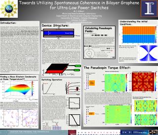
Towards Utilizing Spontaneous Coherence in Bilayer Graphene for Ultra-Low Power Switches M.J. Gilbert Micro and Nanotechnology Laboratory Department of Electrical and Computer Engineering University of Illinois – Urbana-Champaign Urbana, IL 61801 Email: matthewg@illinois.edu Equilibrium Pseudospin Ferromagnet Pseudospin Transfer Torque Transport Orbitals Vinterlayer Singly Occupied Orbitals Δt Δt Eqp Eband Understanding the initial Conditions… Calculating Pseudospin Fields: Introduction: Device Structure: Harnessing collective motion of electrons is a promising approach to creating ultra-low power logic devices . In a switch that is based on a set of independently-moving electrons, switching requires a change in gate voltage large enough to shift each electron’s energy by more than room temperature thermal energy. With collective motion of electrons, one may hope to achieve switching with smaller changes in gate voltage: the energy of an entire ensemble of electrons can be shifted by more than room temperature thermal energy, turning on transport, even though each electron’s energy is shifted by only a small fraction of that amount. One of the most spectacular demonstrations of collective behavior in the last 10 years is the giant enhancement in tunnel current seen in semiconductor bilayer devices in the quantum Hall regime. The enhanced tunnel current between the two layers occurs when electrons in the top layer bind with vacancies in the bottom layer to form “indirect excitons”, which in turn organize into a Bose-Einstein condensate. This type of behavior may be viewed as spontaneous coherence, or “pseudospin ferromagnetism”: selection of a particular superposition of states in the two layers (a particular direction of “pseudospin”, where the layer degree of freedom is treated as if it were a spin) for the entire system. In order for this behavior to be useful in the context of a device, pseudospin ferromagnetism must survive at room temperature, rather than being restricted to cryogenic temperatures as in the GaAs heterostructures in which this effect was discovered. Room temperature operation is possible if the carrier densities in the two layers are equal but with opposite polarity: electrons in one layer, holes in the other. This condition is very difficult to engineer this in a semiconductor system, but could be feasible in graphene. Graphene, a recently discovered form of carbon consisting of a single atomic sheet of graphite, is closely related to graphite, fullerenes and nanotubes, all well-known to both industry and academics. Carbon nanotubes are being explored for use in FETs to extend scaling of conventional charge-based (CMOS) switches. The recent achievement of high quality monolayer graphene with mobilities in excess of 104 cm2 V-1 s-1 suggests that graphene too may be useful for advanced electronics.4 Beyond its remarkable room-temperature mobility, graphene is predicted to have exotic properties due to its unique bandstructure. Most importantly for the present proposal, the carrier density may be tuned through zero – with the same velocity and mobility for electrons and holes – simply by applying a gate voltage5. We propose to develop the theory of spontaneous coherence in bilayer graphene, all with a view toward applications to ultra-low power switching devices. Specifically, we hope to use pseudospin torque and spontaneous interlayer coherence to create a scalable switching device that requires far less energy to switch between low and high conductivity, with equal or better drive current, than optimum MOSFET switching energy predicted by the International Technology Roadmap. Start with the system Hamiltonian: the first term represents the normal kinetic energy operator in the tight binding representation, the second term describes the single particle tunneling amplitude, and the third term describes the electron-electron interactions with φ representing the planar pseudospin field orientation and U as the on-site coulomb interaction term. The ↑ signifies states in the top layer while ↓ signifies the states in the bottom layer. In the ordered state of this system, the quasi-particles in the bilayer have an interlayer tunneling amplitude that contains both a bare single particle tunneling amplitude, Δt, and a self-energy term, Σxc. This self-energy term effectively represents a planar magnetic field which couples to the pseudospins. We now define the expectation value of the self-energy term as where ρ is the system density matrix and σ is a vector of the pauli spin matrices. With this representation, we may now write down the effective planar pseudospin fields ABOVE: Schematic of the proposed device geometry which consists of two monolayers of graphene separated by a tunnel oxide with local gates to control the electron density in the layers separately. Our proposed device consists of two monolayers of graphene separated by a thin insulating tunnel oxide (Fig. 1). The electron densities in the top and bottom monolayers of graphene may be individually tuned by top and bottom gate voltages, VTG and VBG, respectively. By applying a bias Vinterlayer between the top and bottom layers, we will drive a current across the tunnel oxide of thickness d. Experimentally, we would like d ~ 1-5 nm, to achieve a uniform barrier with large tunnel coupling (~ mV). BELOW: Description of the bilayer system in the pseudospin language where the top layer is described as pseudospin ‘up’ and the bottom layer as pseudospin ‘down’ both quantized along the z-direction. Due to the small distance between the layers, the electrons in the top layer are intimately aware of the locations of the vacancies in the bottom layer. The effect that we exploit here is an exchange-correlation (interaction) enhancement of the quasiparticle interlayer tunneling amplitude Δt, by a factor S. The enhancement of the bare tunneling amplitude by interactions is very closely related to the quantum well exchange enhancement effect that has been studied previously using electron gas theory. More specifically, the bare tunneling amplitude combined with the Pauli exclusion principle results in an increased occupation of states with a common inter-layer phase relation. Ns non-local local TOP: The initial electron and hole density for VTG = -VTB = 0.1 V. LEFT: The calculate bandstructure for a 125 nm wide nanoribbon of graphene. and Na Ns – Population of symmetric states Na – Population of anti-symmetric states S - Interlayer exchange enhancement SΔt Fig. 5: (a) Schematic of the bilayer with the top layer lightly doped with electrons and the bottom layer heavily doped with holes. (b) Schematic of the bilayer with equal populations of electrons in the top layer and holes in the bottom. This situation allows spontaneous coherence to form leading to large interlayer currents. The Pseudospin Torque Effect: Electron and Hole Density: Pseudospin Field (Longitudinal Only): eV 0 0 Finding a Bose-Einstein Condensate at Room Temperature?? Switching Operation: Hongki Min et al. arXiv:0802.3462 (2008) y (nm) y (nm) 125 250 0 x (nm) 625 0 x (nm) 625 Here, we show the evolution of the system in equilibrium (TOP) and with an interlayer bias (BOTTOM). In equilibrium, (TOP), since we have composed our wavefunction of +z and –z oriented pseudospin states we may state that the pseudospin polarization is along the +x direction in the plane of the bilayer system. When interlayer bias is smaller than the splitting between the symmetric and anti-symmetric states, the net effective pseudospin field is aligned with the x-direction and this allows the electrons to tunnel more easily from the top layer to the bottom layer. In other words, the transport electrons have yet to produce a torque sufficient to cause the net pseudospin phase angle to anti-align with the transport direction. Therefore, states from the top layer continue to easily precess to the bottom layer, leading to a large tunneling current in the bilayer. As the bias is increased, the Fermi velocity will correspondingly increase in one layer relative to the other layer, resulting in an increase in the net pseudospin phase angle from 0º to 90º, which tells us that the pseudospin phase angle is no longer aligned with the x, or transport, direction, (BOTTOM). At this point, the system switches from a state of high conductivity to a state of low conductivity as the effective pseudospin field produced by the motion of the carriers prevents the carriers from tunneling. This type of operation is analogous to the operation of a Datta-Das transistor9 where the role of the gate voltage used to control the spin precession in narrow gap III-V materials is now played by the interlayer bias. We call this the pseudospin torque effect. We envision that our bilayer graphene switch will operate in much the same way as a typical MOSFET, but with far better subthreshold slope. In our bilayer system, we would set VGB so that the bottom graphene is very heavily hole doped. We then may use VTG to tune the sign of the quasiparticle in the top layer. In Fig. 4, we demonstrate the envisioned Iinterlayer-VTG characteristics for our bilayer switch at an interlayer voltage Vinterlayer < Δt. We begin with VTG = 0, which sets up the situation depicted. In (a). Here there are not many electrons in the top layer and the resultant exchange enhancement between the two layers is small. As VTG is swept to increasingly positive values, more electrons enter the top graphene layer. This increases the interlayer exchange enhancement between the two layers which results in increasingly interlayer currents. We can continue to increase VTG until we reach an electron density in the top layer equal to the hole density in the bottom layer. At this point, the system should undergo spontaneous coherence, shown in (b), and the interlayer current will reach a maximum with a subthreshold slope for our switch ~ S2, potentially with a value far less than the typical 60 mV/decade. e plot the hypothetical Iinterlayer-Vinterlayer characteristics for several different values of VTG. We expect the transfer characteristics to have a very fast rise for applied voltages less than the bare tunnel coupling Δt. When the applied voltage exceeds Δt then the pesudospin torque effect causes the interlayer current to go into saturation resulting in I-V curves very reminiscent of those of a MOSFET. Pseudospin Field (Longitudinal-Top, Transverse-Bottom): eV ABOVE: The critical temperature for coupling between electrons and holes as a function of the electric field applied across the bilayer and the physical separation between the layers. For certain separations and fields, we see that the critical temperature is above room temperature. BELOW: Electron (blue) and hole (red) paths with identical dispersion relations simulated with quantum Monte Carlo. On the left, the density is too low and condensation does not occur. (right) When we cut the domain or equivalently double the density of electrons and holes we see that the paths permute around the domain which is a signature of Bose condensation. 1013 cm-2 Electron and Hole Density: 0 eV y (nm) 250 0 x (nm) 625