Download
1 / 8
80 likes | 176 Vues
Explore methods to shift LVDS voltage levels without chip modifications on SPD VFE board. Investigate feasible solutions for efficient level shifting between boards to optimize power consumption and area space.

E N D
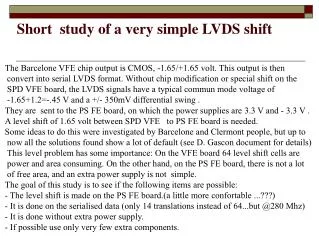
Short study of a very simple LVDS shift The Barcelone VFE chip output is CMOS, -1.65/+1.65 volt. This output is then convert into serial LVDS format. Without chip modification or special shift on the SPD VFE board, the LVDS signals have a typical commun mode voltage of -1.65+1.2=-.45 V and a +/- 350mV differential swing . They are sent to the PS FE board, on which the power supplies are 3.3 V and - 3.3 V . A level shift of 1.65 volt between SPD VFE to PS FE board is needed. Some ideas to do this were investigated by Barcelone and Clermont people, but up to now all the solutions found show a lot of default (see D. Gascon document for details) This level problem has some importance: On the VFE board 64 level shift cells are power and area consuming. On the other hand, on the PS FE board, there is not a lot of free area, and an extra power supply is not simple. The goal of this study is to see if the following items are possible: - The level shift is made on the PS FE board.(a little more confortable ...???) - It is done on the serialised data (only 14 translations instead of 64...but @280 Mhz) - It is done without extra power supply. - If possible use only very few extra components.
Basic ideas The LVDS transmission is current (3.5 mA), fully differential The 350 mV swing is obtained under the 100 Ohms cable load. The receiver is also differential. Thanks to all these points, the idea is to see if the LVDS driver-receiver is capable to make itself this (voltage) level shift. - The driver seems to be able to work up to 4 V power supply: We can gain something like 400-700 mV. - The transmission is current driving: It seems to be possible to biased by 500-1000 mV (?), just by changing the resistive load. To study this, an LVDS output stage was designed with CADENCE IC tools to be able to simulate the effect a self-shift load.
LVDS biased tentative 4 Volts supply : -1.65, +2.35 « T » load at the end of the cable to fix the common mode voltage at 1.2 V (Biased by 1.65 V) Serial resistors to decrease the current in the output transistors.
LVDS-shift result (?) (simulation) Finally the shift of 1.65 Volt is obtained, which gives the classical common mode voltage at the input of the LVDS (1.2 V) To be carefully tested !!!