Download
1 / 42
470 likes | 1.34k Vues
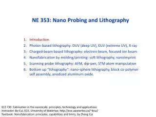
NE 353: Nano Probing and Lithography. Introduction. Photon-based lithography: DUV (deep UV), EUV (extreme UV), X-ray Charged-beam based lithography: electron beam, focused ion beam Nanofabrication by molding/printing: soft lithography, nanoimprint

E N D
NE 353: Nano Probing and Lithography Introduction. Photon-based lithography: DUV (deep UV), EUV (extreme UV), X-ray Charged-beam based lithography: electron beam, focused ion beam Nanofabrication by molding/printing: soft lithography, nanoimprint Scanning probe lithography: AFM, dip-pen, STM atom manipulation Bottom up “lithography”: nano-sphere lithography, block co-polymer self assembly, anodized aluminum oxide. ECE 730: Fabrication in the nanoscale: principles, technology and applications Instructor: Bo Cui, ECE, University of Waterloo; http://ece.uwaterloo.ca/~bcui/ Textbook: Nanofabrication: principles, capabilities and limits, by Zheng Cui
How small is nano? Things Natural Things Manmade 10-2 m 10-3 m Head of a pin1-2 mm Ant ~ 5 mm 10-4 m MicroElectroMechanical Systems (MEMS) 10 -100 micron wide Human hair ~50 micron wide 10-5 m 10-6 m 10-7 m Red blood cells ~ 2-5 micron 10-8 m Nanorobot Au nanoparticles 13 nm & 50 nm Intel transistor Virus, ~100nm 10-9 m DNA ~2 nm diameter Carbon nanotube ~2 nm diameter 10-10 m Adapted from office of Basic Energy Sciences Office of Science Micro world Nano world (1-100nm)
Why go to nano? L: length • Integrated circuit: faster, more function, lower power consumption • Data storage: higher capacity (1/L2), 1Tbits/in2 – 25nm25nm/bit • Semiconductor: quantum confined phenomena (quantum dots/wells…) • Magnetism: single domain formation at • L<magnetic domain wall thickness, super-paramagnetism • Photonics: new phenomena at L< • photonic crystal, negative refractive index, near field optics, plasmonics • Biomedical: DNA sorting (nanofluidics), drug delivery (nanoparticles), bio-sensors • Chemistry: higher surface area • higher reactivity for catalyst, higher sensitivity for chemical sensors
Nanofabrication - two principal approaches Top Down: Implementation of various techniques to remove, add or redistribute atoms or molecules in a bulk material to create a final structure. Miniaturizing existing processes at the macro/micro/nano-scale Bottom up: Atomic and molecular (or larger) scale directed assembly to create larger scale structures with engineered properties E.g. chemical self -assembly Machined Assembled
Top-down nanofabrication Top down approach: three components Lithography (lateral patterning):generate pattern in a material called resist photolithography, electron-beam lithography, nanoimprint lithography… Thin film deposition (additive):spin coating, chemical vapor deposition, molecular beam epitaxy, sputtering, evaporation, electroplating… Etching (subtractive): reactive ion etching, ion beam etching, wet chemical etching, polishing…
Top down nanofabrication: one example metal nanostructures Metal nanostructures side view substrate substrate Direct etch process Liftoff process resist (polymer) resist (polymer) 1. Thin film growth 1. Thin film growth 2. Lithography 2. Lithography 3. Etching 3. Deposition 4. Etching (dissolve resist) 4. Etching (dissolve resist)
35 nm diameter 70 nm diameter 115 nm diameter One more step: pillar array with various diameters Pitch: 200nm Cr silicon 1. Cr dots by liftoff 2. RIE silicon and remove Cr (RIE: reactive ion etching)
Pattern transfer (next step after lithography) or doping Direct etch Electroplating… Liftoff
Reticle (Mask) Wafer 193 nm Excimer Laser Source Exposure Column (Lens) Computer Console How lithography started State-of-art lithography tool for IC industry • Lithography (Greek for "stone drawing"); based on repulsion of oil and water. • Invented by AloisSenefelder in 1798. • Used for book illustrations, artist's prints, packaging, posters, etc. • In 1825, Goya produced a series of lithographs. • In the 20th century, it become an important technique with unique expressive capabilities in the art field. • Nowadays used in semiconductor manufacturing and micro-nanofabrication.
Key requirements of lithography • Critical dimension (CD) control • Size of features must be controlled within wafer and wafer-to-wafer • Overlay (alignment between different layers) • For high yield, alignment must be precisely controlled • Defect control • Other than designed pattern, no additional patterns must be created • Low cost • 30-40% of total semiconductor manufacturing cost is due to lithography (masks, resists, metrology) • At the end of the roadmap, micro-processor will require 39 mask levels • Therefore, lithography is the most important part of semiconductor industry, as well as of fabrication micro/nano-devices for R&D.
Introduction. Photon-based lithography: DUV (deep UV), EUV (extreme UV), X-ray Charged-beam based lithography: electron beam, focused ion beam Nanofabrication by molding/printing: soft lithography, nanoimprint Scanning probe lithography: AFM, dip-pen, STM atom manipulation Bottom up “lithography”: nano-sphere lithography, block co-polymer self assembly, anodized aluminum oxide.
Optical/UV lithography (= photolithography) • Process used to transfer a pattern from a photomask to the surface of a substrate • Formation of images with visible or ultraviolet radiation in a photoresist • No limitation of substrate (Si, glass, metal, plastic...) • Working horse of current chip manufacturing processes (45nm feature size) • For R&D, it is the most widely used lithography system, but with 1m feature size, so only for micro-fabrication. • Block radiation where it is not wanted, i.e. absorb radiation • Need opaque material at the desired wavelength • Transmit radiation where it is needed • Need material with high transmission at the desired wavelength • For optical lithography, mask is quartz glass (transparent) + Cr (opaque)
Three optical lithography methods Contact aligner Proximity aligner Projection aligner Mask in contact with photo-resist film (Gap 0 m) Gap (order 10m) between mask photoresist Like photography, imaging
Projection printing Rayleigh resolution: Numerical aperture, NA • Similar to photography: image formation on the resist surface • Resolution is limited by far field diffraction (Fraunhofer), need good lens for high resolution. • Usually print small area (e.g. ¼ reduction), then step and repeat. • Very expensive, used mainly by semiconductor industry, unpopular for academic research. • Currently, IC industry uses =193nm deep UV light from ArF excimer laser (10s nano-second incoherent pulse) for exposure, with resolution (half-pitch of dense line array) 45nm.
Extreme ultraviolet (EUV) lithography (=13.5nm) • Short wavelength (13.5 nm) permits high resolution even with small numerical apertures. • One candidate for next generation lithography EUV mirror Lens (transmission) is not possible at EUV. So use reflection lens (mirrors). Bragg reflector made of alternating Mo/Si layers that enables high efficiency (68% at normal incidence) reflection of 13.5 nm light.
X-ray lithography (XRL) Incident x-rays Mask (membrane and patterned absorber) Frame (glass..) Resist Gap Wafer • λ1nm (extremely short wavelength for high resolution). • X-rays are produced by synchrotron radiation in a high energy electron storage ring. • Contamination becomes a smaller concern because X-rays will penetrate most dust particles (low atomic number). • No need for vacuum (little absorption of x-ray by air). • No lens (transmission or reflection), because for X- ray, refractive index n1; thus only proximity printing. • Proximity printing can still achieve high resolution (<30nm) due to small λ. (R>>; g is gap, order 1m; t is film thickness, order 100nm) Resolution:
X-ray lithography for high aspect ratio and 3D Deep penetrating power of the x-rays into the photoresist and low diffraction (spread of beam), thus good for creating microstructures with great height (high aspect ratio). High aspect ratio micro-structures Intersection of the three beams Three-cylinder photonic crystal structure in ceramic. Exposed by repeated exposures at different tilt angles between the mask and synchrotron. Almost like mechanical drilling. G. Feiertag, APL, 71 (11) 1997. 80μm resist structure with aspect ratio > 10. White, APL, 66 (16) 1995.
Introduction. Photon-based lithography: DUV (deep UV), EUV (extreme UV), X-ray Charged-beam based lithography: electron beam, focused ion beam Nanofabrication by molding/printing: soft lithography, nanoimprint Scanning probe lithography: AFM, dip-pen, STM atom manipulation Bottom up “lithography”: nano-sphere lithography, block co-polymer self assembly, anodized aluminum oxide.
Electron beam lithography (EBL) Finely focused electron beam, =2-5nm Resist (PMMA…) Metal patterning by EBL and liftoff
Electron beam lithography (EBL) • Electron beam has a wavelength so small that diffraction is insignificant. • Tool is just like an SEM with on-off capability controlled by a “beam blanker”. • Accurate positioning (alignment): “see” the substrate first, then expose. • Beam spot diameter of 2nm can be achieved, at typical acceleration voltage of >20keV. • But typical resolution 15nm (>> beam diameter), limited by proximity effect and lateral diffusion of secondary electrons. • Most popular prototyping tool for R&D, but too slow for mass production. Wavelength of electrons Where V is electron energy in eV unit. For example, 30keV → =0.007nm!
Focused ion beam (FIB) • Ga+ ion beam (down to 5nm) to raster scan over the surface. • FIB can cut away (mill, sputter) material (electron is too light for this). • By introducing gases, FIB can selectively etch or deposit a metal or oxide.
Focused ion beam (FIB) • Like electron beam lithography (EBL), direct write technique – no mask necessary. • Can expose a resist with higher sensitivity than EBL, but very low penetration depth. • In principle, FIB has better resolution than e-beam lithography because secondary electrons have lower energy (but it is easier to focus electron beams). • Re-deposition of sputtered material to other part of the device is a problem. • In summary, very versatile (deposition, etching, lithography, all in one tool); but slow and expensive, more complicated than EBL. A FIB system is similar to SEM, but ion source is used to replace electron source. Most lab systems have both ion source and electron source (dual beam). SIM: scanning ion microscopy, similar to SEM except that now the secondary electrons (signal to form image) is generated by ion – matter interaction.
Introduction. Photon-based lithography: DUV (deep UV), EUV (extreme UV), X-ray Charged-beam based lithography: electron beam, focused ion beam Nanofabrication by molding/printing: soft lithography, nanoimprint Scanning probe lithography: AFM, dip-pen, STM atom manipulation Bottom up “lithography”: nano-sphere lithography, block co-polymer self assembly, anodized aluminum oxide.
Soft lithography: molding, printing, material transferring Why it is called soft lithography? Because no energetic beams (electron, ion) or radiations (DUV, x-ray) are involved. Stamp (mold) production • A master mold is made by lithographic techniques and a stamp is cast from this master. • Poly di-methyl siloxane (PDMS) is most popular material for stamps. PDMS stamp (mold) after peel off from SU-8 master Photolithography pattern SU-8 Cast PDMS pre-polymer and cure
Soft-lithography I: micro-contact printing (μCP) • Minimum resolution affected by diffusion of molecules, can reach sub-50nm. • PDMS is deformable – can accommodate rough surfaces or spherical substrates. • Self assembled mono-layers (SAM) are efficient barriers against chemical etches. • For example, SAM monolayer can be used as etching mask to pattern Au using wet-etch.
Soft lithography II: micro-molding in capillaries (MIMIC) • PDMS mold is placed directly on top of the substrate and pre-polymer is placed at the open ends of the channel. • Due to the capillary effect, the pre-polymer completely fills in the channels of the stamp. • After the pre-polymer has filled the channels of the PDMS mold, it is cured (become solid, by UV light or baking). • Can be used with UV- curable prepolymers, inorganic salts, colloidal particles, and other materials Liquid pre-polymer
Nanoimprint lithography (thermal/hot embossing) mold Heat-up polymer resist and press down Cool-down and remove mold Pattern transfer to substrate Mold = mask = template = stamp
UV-curing nanoimprint lithography (Au patterning by liftoff as an example) • Liquid resist, soft and deformable by mold. • Hardened by UV-curing (polymerization). • Molds must be transparent (PDMS, Quartz). • No temperature (thermal cycle) necessary. • Thus a very gentle process, and thermal expansion mismatch no longer an issue.
Introduction. Photon-based lithography: DUV (deep UV), EUV (extreme UV), X-ray Charged-beam based lithography: electron beam, focused ion beam Nanofabrication by molding/printing: soft lithography, nanoimprint Scanning probe lithography: AFM, dip-pen, STM atom manipulation Bottom up “lithography”: nano-sphere lithography, block co-polymer self assembly, anodized aluminum oxide.
Scanning probe lithography (also termed “tip-based nanofabrication”) • Mechanical patterning: scratching, nano-indentation • Chemical and molecular patterning (dip-pen nanolithography, DPN) • Voltage bias application • Field enhanced oxidation (of silicon or metals) • Electron exposure of resist materials • Manipulation of atoms/molecules by STM, or nanostructures by AFM AFM: atomic force microscopy (X-Y positioning by piezo; Z deflection by optical measurement)
AFM lithography – indentation and scratching (simplest, mechanical lithography) • Material is removed from the substrate leaving deep trenches with the characteristic shape of the tip used. • The advantages of nano-scratching for lithography • Precision of alignment, see using AFM imaging, then pattern wherever wanted. • The absence of additional processing steps, such as etching the substrate. • But it is not a clean process (debris on wafer), and the AFM tip cannot last long.
Dip-pen nanolithography (DPN) • Similar to micro-contact printing, writing using a “fountain pen”. • AFM tip is “inked” with material to be deposited • Sub-15nm features demonstrated • Multiple DPN tip arrays for higher throughput production
AFM lithography: oxidation (local electrochemical anodization) The high field desorbs the hydrogen on the silicon surface and enables exposed silicon to oxidize in air. Oxidation rate is further enhanced by the high electric field. • Resulting oxide affected by experimental parameters • Voltage (typically from 5-10V) • Tip scan speed (stationary to tens of µm/s) • Humidity (20% to 80%)
STM lithography (STM: scanning tunneling microscopy) • By applying a voltage between tip and substrate it is possible to deposit or remove atoms or molecules. • Advantages of STM Lithography • Information storage devices (one atom per bit, highest storage density possible). • Nanometer patterning technique (highest resolution, Å). Iron atoms on copper (111) substrate
Summary: lithography – general distinction • Lithography on surfaces • Optical/UV lithography • E-beam lithography • FIB lithography • X-ray lithography • SPM-lithography • Imprint lithography • Stencil mask lithography • Lithography in volume • Two photon absorption • Stereo-lithography • Lithography with particles or waves • Photons: photolithography • X-rays: from synchrotron, x-ray lithography • Electrons: electron beam lithography (EBL) • Ions: focused ion beam (FIB) lithography • Imprint lithography (molding) • Soft lithography: micro-contact-printing… • Hot embossing • UV-curing imprinting • SPM-lithography • AFM • STM • DPN (dip-pen nanolithography) • Pattern replication: parallel • (masks/molds necessary) • High throughput, for manufacturing, not easy to change pattern • Optical lithography • X-ray lithography • Imprint lithography • Stencil mask lithography • Pattern generation: serial • (Slow, for mask/mold making or R&D) • E-beam lithography (EBL) • Ion beam lithography (FIB) • SPM-lithography • Multiple serial (array) • Electron-beam micro-column array (arrayed EBL) • Zone plate array lithography • Scanning probe array
Introduction. Photon-based lithography: DUV (deep UV), EUV (extreme UV), X-ray Charged-beam based lithography: electron beam, focused ion beam Nanofabrication by molding/printing: soft lithography, nanoimprint Scanning probe lithography: AFM, dip-pen, STM atom manipulation Bottom up “lithography”: nano-sphere lithography, block co-polymer self assembly, anodized aluminum oxide.
Bottom-up nanofabrication • Low cost, high resolution (few nm), 3D (sphere) • Chemical synthesis • Nanotubes, nanowires, nano…any shape • Quantum dots and nanoparticles • Functional arrangement • Self assembly • Mono-layers, e.g. nano-sphere lithography • Block copolymers • Functionalized nanoscale structures • Fluidic or field assisted assembly • Surface tension directed assembly • Templated growth, guided assembly • Step edges and defect or strain fields • Porous materials, e.g. anodized aluminum oxide Carbon nanotube Anodized aluminum oxide
Phase separation of block copolymers Phase separation of a blend of PMMA and PS homo-polymer A blend of two incompatible homo-polymer separates into distinct phases on a large scale (left), whereas block copolymers separate into periodic domains (right). Basic morphologies obtained by different block copolymer compositions. PMMA: poly(methyl methacrylate) PS: polystyrene Ma, “Fabrication of super-hydrophobic film from PMMA with intrinsic water contact angle below 90o”, Polymer, 48, 7455-7460 (2007).
Phase separation of block copolymers Tapping mode atomic force microscopy images of PS-PHMA self assembly on top of -Si /SiO2 substrate: Quiescently annealed Shear aligned. Glassy PS cylinders are shown as light in a dark rubbery PHMA matrix. Polystyrene-b-poly(n-hexylmethacrylate) (PS–PHMA) diblock copolymer with a molar mass of 21 and 64 kg/mol for the respective blocks. Alignment by shear force Chaikin, “Silicon nanowire grid polarizer for very deep ultraviolet fabricated from a shear-aligned diblock copolymer template”, Optics letters, 32(21), 3125-3127 (2007). Pitch=30nm
Anodized aluminum oxide (AAO) 2Al + 3H2O → Al2O3 + 3H2 [G = -8.65 105J] • Anodization: • A direct current is passed through an electrolytic solution where the Al sheet is used as the anode. • Two processes: dissolving and oxidation • Naturally formed triangular pore arrays Electrolyte: Oxalic acid, phosphoric acid, sulfuric acid …
AAO membrane production Al2O3 Al Free standing 10m-thick AAO membrane, with Au plated for better viewing contrast.