Lecture #5 – VLSI Design Review
300 likes | 587 Vues
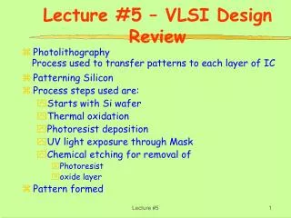
Lecture #5 – VLSI Design Review. Photolithography Patterning Silicon Process steps used are: Starts with Si wafer Thermal oxidation Photoresist deposition UV light exposure through Mask Chemical etching for removal of Photoresist oxide layer Pattern formed.

Lecture #5 – VLSI Design Review
E N D
Presentation Transcript
Lecture #5 – VLSI DesignReview • Photolithography • Patterning Silicon • Process steps used are: • Starts with Si wafer • Thermal oxidation • Photoresist deposition • UV light exposure through Mask • Chemical etching for removal of • Photoresist • oxide layer • Pattern formed Process used to transfer patterns to each layer of IC Lecture #5
Polysilicon Gate Field Oxide (Thick Oxide) Gate Oxide (Thin Oxide) NMOS Transistor Lecture #5
Patterning Silicon Si - Substarate Silicon Di-oxide Lecture #5
Photoresist Oxide Layer Silicon Wafer Process steps for Patterning Grow Crystal Saw Bare silicon Wafer 4-12” dia <1mm Silicon Wafer Thermal Grow Oxide Layer Oxidation SiO2 1m Oxide Layer Silicon Wafer Spin coating with Photoresist –1mm Light Sensitive organic polymer Acid-resistant Soluble once exposed to UV Light Lecture #5
Oxide Layer Silicon Wafer Pattern formed on a glass plate (Mask) Transparent & Opaque regionsPositive Photoresist Non exposed regions hardened higher resolution Expose to Ultraviolet Light Exposed soluble (hardened) Lecture #5
Soluble photoresist is chemically removed (etching) using HF acid Oxide Layer Silicon Wafer Silicon Wafer Silicon Wafer Etching continued to remove SiO2 High-temp. plasma removes hardened photoresist Pattern formed Lecture #5
Si - Substarate Patterned Silicon Lecture #5
(l) Lecture #5
n-well CMOS Process Lecture #5
The CMOS Process – Photolithography (1) Grow Crystal Saw Lecture #5
The CMOS Process – Photolithography (2) Lecture #5
Mask 1: N-well Diffusion Impurity Implantation Lecture #5
Mask 2: Define Active Regions Lecture #5
Mask 3: Polysilicon Gate Lecture #5
Mask 4: n+ Diffusion Lecture #5
Mask 5: p+ Diffusion Lecture #5
Mask 6: Contact Holes Lecture #5
Mask 7: Metallization Lecture #5
Cross Section of a CMOS Inverter Lecture #5
Vdd S N-Well P-Channel L G D W IN OUT P-Substrate D N-Channel L G S GND Lecture #5
Layout of CMOS ICs Translating the circuit schematic into a set of patterned layers in a silicon substrate Layout drawings are used to generate the masks needed for fabrication Every layer is described by geometrical objects of specified shape and size obeying certain rules (Design Rules). Each layer is described by a distinct color Lecture #5
Why do we need design rules? • Masks are tooling for manufacturing. • Manufacturing processes have inherent limitations in accuracy. • Design rules specify geometry of masks which will provide reasonable yields. • Design rules are determined by experience • Design rule violation may result in a non-functional circuit Lecture #5
Manufacturing Problems • Photoresist shrinkage, tearing. • Variations in material deposition. • Variations in temperature. • Variations in oxide thickness. • Impurities. • Variations between lots. • Variations across a wafer. Lecture #5
Transistor Problems • Variations in threshold voltage: • oxide thickness; • ion implantation; • poly variations. • Changes in source/drain diffusion overlap. • Variations in substrate. Lecture #5
Wiring problems • Diffusion: changes in doping -> variations in resistance, capacitance. • Poly, metal: variations in height, width -> variations in resistance, capacitance. • Shorts and opens: Lecture #5
Oxide problems • Variations in height. • Lack of planarity -> step coverage. metal 2 metal 2 metal 1 Lecture #5
Via Problems • Via may not be cut all the way through. • Undersized via has too much resistance. • Via may be too large and create short. Lecture #5
