Download
1 / 13
130 likes | 229 Vues
Discover the potential of molecular plasmonics at the intersection of photonics, chemistry, and nanotechnology for diverse applications in sensors and photonics.

E N D
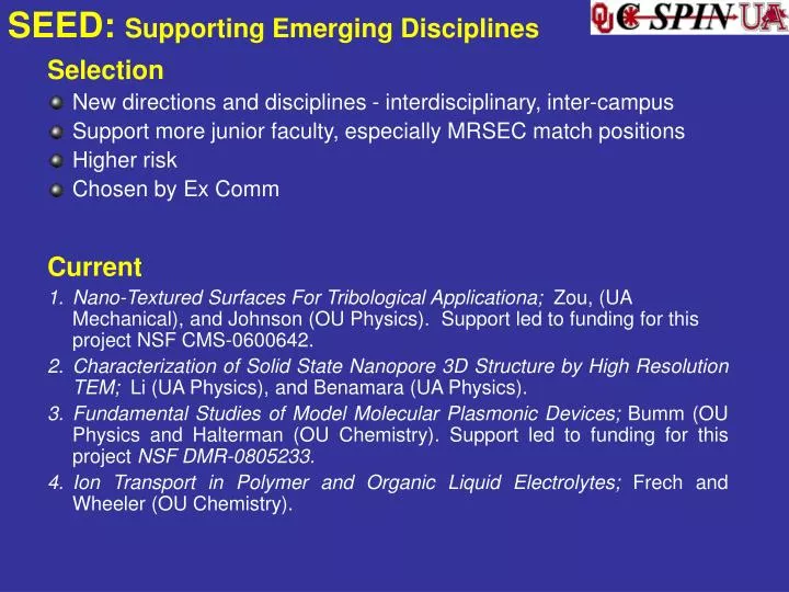
SEED: Supporting Emerging Disciplines Selection • New directions and disciplines - interdisciplinary, inter-campus • Support more junior faculty, especially MRSEC match positions • Higher risk • Chosen by Ex Comm Current • Nano-Textured Surfaces For Tribological Applicationa;Zou, (UA Mechanical), and Johnson (OU Physics). Support led to funding for this project NSF CMS-0600642. • Characterization of Solid State Nanopore 3D Structure by High Resolution TEM; Li (UA Physics), and Benamara (UA Physics). • Fundamental Studies of Model Molecular Plasmonic Devices; Bumm (OU Physics and Halterman (OU Chemistry). Support led to funding for this project NSF DMR-0805233. • Ion Transport in Polymer and Organic Liquid Electrolytes; Frech and Wheeler (OU Chemistry).
Fundamental Studies of Model Molecular Plasmonic Devices Scattered LightCollection Dark-FieldIllumination Sample 939 nm 1252 nm 714 nm 617 nm 1000 nm 654 nm 150 nm DARK-FIELDMicroscope Objective 100x NA 0.9 Motivation • Molecular plasmonics is an emerging field of scientific investigation at the intersection of photonics, chemistry, and nanotechnology. • Photonic energy can be manipulated with subwavelength control and interact with adsorbed molecules. Objective • Explore the interaction of adsorbed dyes with nanoparticle plasmon resonances and their plasmon mediated interactions with spatially remote dyes. • Explore site specific surface chemistry for controlling dye location on the nanometer scale. Significance • The results will provide guidelines for the rationale design of molecular plasmonic systems. • Broad range of potential applications: photonics, sensors, and many other applications. Discrete-Dipole Approximation (DDA) calculation FGNP on ITO substrate Achermann, et al., Optics Lett.32, 2254 (2007). NSF DMR grant funded (DMR-0805233): Fundamental Studies of Model Molecular Plasmonic Devices, Halterman and Bumm
Optical Absorption SpectroscopyMalachite Green Adsorbed on Gold Nanoparticles before MG with MG MG Measure light scattering before and after dye adsorption. • Measured optical absorption is constant with adsorbate coverage estimates. • Possible surface enhanced optical absorption. How many molecules? by optical absorptionε = 1.5×10⁴n = 170 zmole by adsorption geometry Standing up, edge onA = ~6.0×10⁻¹⁵n = 200 zmole Lying flat up, edge onA = ~1.2×10⁻¹³n = 10 zmole zeptomoles of MG (1 zmole≈ 600 molecules)
Site Specific Surface Chemistry w/ STMCatalytic azide-alkyne “Click” chemistry azide + alkyne1,2,3-triazole link catalyst 50 nm × 50 nm STM image 100 nm × 100 nm STM image Decanethiol HS(CH2)9CH3 Azide islands HS(CH2)10N3 Molecular sitesreacted with alkynep-CH3C6H4CCH AFTER REACTION BEFORE REACTION
Exploring New Methods for Sequencing Single DNA Molecules Biomolecule translocation experiments show a relationship between the current drop, ΔIb, and nanopore thickness, H. Ohmic Conductor: Signal: Research Goal: Use ion beam sculpting parameters to fabricate thinner and low noise nanopores.
Nanopore Sculpting with Different Ion Species Nanopore Sculpting with different ion species results in different closing rates. Helium exhibits the slowest closing rate, thereby giving the most control over the final pore diameter.
Nanopore Characterization using Electron Energy Loss Spectra (EELS) STEM image with position numbers Initial EELS taken at two positions near the nanopore to help estimate the thickness profile of the nanopore. Data taken in collaboration OU EELS thickness study completed at UA with Benamara
Nano-Textured Surfaces for Tribological Applications http:/www.seagate.com Surface with micro-dimples textured by laser. Ni Nanodot-Patterned Surface (NDPS) RF-MEMS adhered to the substrate. Optical micrograph of laser-textured zone on the magnetic hard drive disk surface.
Nickel Nanodot-Patterned Surfaces (NDPSs) 100 nm Ni {200} Ni {111} NiO {111} Size of NBD beam (70 nm) 50 nm Si {220} Ordered array of Ni nanodots: Fabricated by evaporating Ni through an anodized aluminum oxide (AAO) mask. Top-down and oblique-angle SEM images of Ni NDPS. AFM and SEM allow characterization of the dots and dot array. TEM allows characterization of the crystallinity. TEM characterization of Ni NDPS shows the polycrystalline nature of the dots
Mechanical Properties of Ni NDPSs 400 nm Load vs. Displacement Curves Three load–displacement curves for a 70 μN indentation load. AFM (left) and SEM (right) images of a nano-indented array for a 500 μN indentation test. Hardness & Contact Area vs. Load Elastic modulus of Ni nanodots is 160 ± 20 GPa, which is less than bulk nano or micro crystalline Ni (186 and 204 GPa, respectively). Hardness is 7.7 ± 1.0 GPa, in agreement with that of nanocrystalline Ni (8 GPa), but larger than that of microcrystalline Ni (3 GPa).
Tribological Properties of Ni NDPS Coefficient of friction for Ni NDPS and smooth Si(100) - 80% reduction at low loads. Correlation between surface topography and the signatures in the lateral force vs. lateral displacement curve for a 0–200 mN scratch Friction is proportional to contact area at nanoscale. The critical shear strength of the Ni nanodots/Si substrate interface was estimated to be about 1.24 GPa. In the process of developing a friction model for NDPS. Adhesion force for Ni NDPSs and smooth Si(100)- up to 90% reduction.
Modeling of Indentation on Ni NDPS Integrate into multi-asperity contact model. Finite Element Analysis of single asperity contact. Modeling results are in good agreement with experimental results. The model can thus be used as a design tool for NDPS systems.
Indentation on Flat Gold Nanoparticles 5.5 μN (150 nm) 5.5 μN (150 nm) 500 nm 500 nm 11 μN (300 nm) 11 μN (300 nm) Flat gold nanoparticles (FGNPs) are high-quality single-crystal particles with micron lateral dimensions and 20 to 50 nm thick. They are ideally suited to study the generation of dislocation networks etc. under nanoindention. To see damage, from nano-indentation, we must use the TEM to characterize FGNP before & after indention. This requires the FGNPs to be on ultra-thin TEM grids. Here we demonstrate the technique using 50 nm thick Si3N4 grids. Bright-field (BF) TEM image of indented FGNP. Indentation areas enclosed by red circle with indentation force labeled. (202) dark-field (DF) TEM image of indented FGNP. Indentation areas enclosed by red circle with indentation force labeled. In this preliminary work, individual dislocations within dislocation networks are clearly seen with BF and DF TEM.