Lecture 1 Op-Amp
Lecture 1 Op-Amp. Introduction of Operation Amplifier (Op-Amp) Analysis of ideal Op-Amp applications Comparison of ideal and non-ideal Op-Amp Non-ideal Op-Amp consideration. Operational Amplifier (Op-Amp). Very high differential gain High input impedance Low output impedance

Lecture 1 Op-Amp
E N D
Presentation Transcript
Lecture 1 Op-Amp • Introduction of Operation Amplifier (Op-Amp) • Analysis of ideal Op-Amp applications • Comparison of ideal and non-ideal Op-Amp • Non-ideal Op-Amp consideration Operational Amplifier
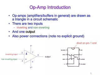
Operational Amplifier (Op-Amp) • Very high differential gain • High input impedance • Low output impedance • Provide voltage changes (amplitude and polarity) • Used in oscillator, filter and instrumentation • Accumulate a very high gain by multiple stages Operational Amplifier
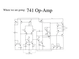
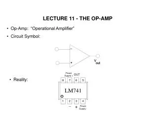
IC Product DIP-741 Dual op-amp 1458 device Operational Amplifier
Single-Ended Input • + terminal : Source • – terminal : Ground • 0o phase change • + terminal : Ground • – terminal : Source • 180o phase change Operational Amplifier
Double-Ended Input • Differential input • 0o phase shift change • between Vo and Vd Qu: What Vo should be if, Ans: (A or B) ? (A) (B) Operational Amplifier
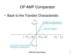
Distortion The output voltage never excess the DC voltage supply of the Op-Amp Operational Amplifier
Common-Mode Operation • Same voltage source is applied • at both terminals • Ideally, two input are equally • amplified • Output voltage is ideally zero • due to differential voltage is • zero • Practically, a small output • signal can still be measured Note for differential circuits: Opposite inputs : highly amplified Common inputs : slightly amplified Common-Mode Rejection Operational Amplifier
Common-Mode Rejection Ratio (CMRR) Differential voltage input : Common voltage input : Common-mode rejection ratio: Output voltage : Note: When Gd >> Gc or CMRR Vo = GdVd Gd : Differential gain Gc : Common mode gain Operational Amplifier
CMRR Example What is the CMRR? Solution : (2) (1) NB: This method is Not work! Why? Operational Amplifier
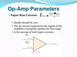
Op-Amp Properties • Infinite Open Loop gain • The gain without feedback • Equal to differential gain • Zero common-mode gain • Pratically, Gd = 20,000 to 200,000 • (2) Infinite Input impedance • Input current ii ~0A • T- in high-grade op-amp • m-A input current in low-grade op-amp • (3) Zero Output Impedance • act as perfect internal voltage source • No internal resistance • Output impedance in series with load • Reducing output voltage to the load • Practically, Rout ~ 20-100 Operational Amplifier
Frequency-Gain Relation • Ideally, signals are amplified from DC to the highest AC frequency • Practically, bandwidth is limited • 741 family op-amp have an limit bandwidth of few KHz. 20log(0.707)=3dB • Unity Gain frequency f1: the gain at unity • Cutoff frequency fc: the gain drop by 3dB from dc gain Gd GB Product : f1 = Gdfc Operational Amplifier
? Hz 10MHz GB Product Example: Determine the cutoff frequency of an op-amp having a unit gain frequency f1 = 10 MHz and voltage differential gain Gd = 20V/mV • Sol: • Since f1 = 10 MHz • By using GB production equation • f1 = Gdfc • fc = f1 / Gd = 10 MHz / 20 V/mV • = 10 106 / 20 103 • = 500 Hz Operational Amplifier
Ideal Vs Practical Op-Amp Operational Amplifier
Ideal Op-Amp Applications Analysis Method : Two ideal Op-Amp Properties: • The voltage between V+ and V is zero V+ = V • The current into both V+ and V termainals is zero For ideal Op-Amp circuit: • Write the kirchhoff node equation at the noninverting terminal V+ • Write the kirchhoff node eqaution at the inverting terminal V • Set V+ = V and solve for the desired closed-loop gain Operational Amplifier
Noninverting Amplifier • Kirchhoff node equation at V+ yields, • Kirchhoff node equation at Vyields, • Setting V+ = V– yields • or Operational Amplifier
Noninverting amplifier Noninverting input with voltage divider Less than unity gain Voltage follower Operational Amplifier
Inverting Amplifier • Kirchhoff node equation at V+ yields, • Kirchhoff node equation at Vyields, • Setting V+ = V– yields Notice: The closed-loop gainVo/Vin is dependent upon the ratio of two resistors, and is independent of the open-loop gain. This is caused by the use of feedback output voltage to subtract from the input voltage. Operational Amplifier
Multiple Inputs • Kirchhoff node equation at V+ yields, • Kirchhoff node equation at Vyields, • Setting V+ = V– yields Operational Amplifier
Inverting Integrator • Now replace resistors Ra and Rf by complex components Za and Zf, respectively, therefore • Supposing • The feedback component is a capacitor C, i.e., • The input component is a resistor R, Za = R • Therefore, the closed-loop gain (Vo/Vin) become: • where • What happens if Za = 1/jC whereas, Zf = R? • Inverting differentiator Operational Amplifier
Op-Amp Integrator • Example: • Determine the rate of change • of the output voltage. • Draw the output waveform. Solution: (a) Rate of change of the output voltage (b) In 100 s, the voltage decrease Operational Amplifier
Op-Amp Differentiator Operational Amplifier
Non-ideal case (Inverting Amplifier) Equivalent Circuit • 3 categories are considering • Close-Loop Voltage Gain • Input impedance • Output impedance Operational Amplifier
Close-Loop Gain Applied KCL at V– terminal, By using the open loop gain, The Close-Loop Gain, Av Operational Amplifier
Close-Loop Gain When the open loop gain is very large, the above equation become, Note : The close-loop gain now reduce to the same form as an ideal case Operational Amplifier
Input Impedance can be regarded as, where R is the equivalent impedance of the red box circuit, that is However, with the below circuit, Input Impedance Operational Amplifier
Input Impedance Finally, we find the input impedance as, Since, , Rin become, Again with Note: The op-amp can provide an impedance isolated from input to output Operational Amplifier
Output Impedance Only source-free output impedance would be considered, i.e. Vi is assumed to be 0 Firstly, with figure (a), By using KCL,io = i1+ i2 By substitute the equation from Fig. (a), R and A comparably large, Operational Amplifier