Transport experiments on topological insulators
340 likes | 850 Vues
Transport experiments on topological insulators. J. Checkelsky, Dongxia Qu, Qiucen Zhang, Y. S. Hor, R. J. Cava, NPO. Magneto-fingerprint in Ca-doped Bi2Se3 Tuning chemical potential in Bi2Se3 by gate voltage Transport in non-metallic Bi2Te3. Supported by NSF DMR 0819860.

Transport experiments on topological insulators
E N D
Presentation Transcript
Transport experiments on topological insulators J. Checkelsky, Dongxia Qu, Qiucen Zhang, Y. S. Hor, R. J. Cava, NPO • Magneto-fingerprint in Ca-doped Bi2Se3 • Tuning chemical potential in Bi2Se3 by gate voltage • Transport in non-metallic Bi2Te3 Supported by NSF DMR 0819860 Exotic Insulator conf. JHU Jan 14-16, 2010 November 19, 2009
Quantum oscillations of Nernst in metallic Bi2Se3 Problem confronting transport investigation As-grown xtals are always excellent conductors, m lies in conduction band (Se vacancies). r (1 K) ~ 0.1-0.5 mWcm, n ~ 1 x 1018 cm-3 m* ~ 0.2, kF ~ 0.1 Å-1
Resistivity vs. Temperature : In and out of the gap Checkelsky et al., PRL ‘09 Onset of non-metallic behavior ~ 130 K SdH oscillations seen in both n-type and p-type samples Non-metallic samples show no discernable SdH
Metallic vs. Non-Metallic Samples: R(H) R(H) profile changes below T onset of non-metallic behavior Low H feature develops below 50 K Metallic samples display positive MR and detectable SdH oscillations
Low H behavior At lower T, low H peak in G(H) becomes more prominent Consistent with sign for anti-localization
Non-Metallic Samples in High Field Fluctuation does not change character significantly in enhanced field Still no SdH oscillations
Magnetoresistance of gapped Bi2Se3 Checkelsky et al., PRL ‘09 Giant, quasi-periodic, retraceable conductance fluctuations Conductance fluctuations Logarithmic anomaly
Magneto-fingerprints Checkelsky et al., PRL ‘09 Fluctuationsretraceable Giant amplitude (200-500 X too large) Retraceable (fingerprints) Spin degrees Involved in fluctuations
Quasi-periodic fluctuations Background removed with T = 10 K trace (checked with smoothing) Autocorrelation C should polynomial decrease for UCF yielding If interpreted as Aharonov-Bohm effect, Fourier components yield
Table of parameters non-metallic Bi2Se3 Checkelsky et al., PRL ‘09 Signal appears to scale with G but not n Possibly related to defects that cause conductance channels Thickness dependence obscured by doping changes?
Angular Dependence of R(H) profile Cont. Checkelsky et al., PRL ‘09 For δG, 29% spin term For ln H, 39% spin term (~200 e2/h total) Theory predicts both to be ~ 1/2π (Lee & Ramakrishnan), (Hikami, Larkin, Nagaoka)
Quasi-periodic fluctuations vs T Fluctuation falls off quickly with temperature For UCF, expect slow power law decay ~T-1/4 or T-1/2 AB, AAS effect exponential in LT/P Doesn’t match!
Features of anomalous magneto-fingerprint • Observed in mm-sized xtals – not UCF • RMS value very large 1-10 e2/h • Modulated by in-plane (spin degrees play role) • T dependence steeper than UCF
Young & Kim, Nat. Phys 2008 Fabry-Perot resonances produce cond. oscillationsof amplitude 5-10 e2/h
Bismuth Telluride Non-metallic samples Bi2Te3 Bi2Se3
Cleaved Crystals 28 Ǻ 2 µm
Tune carrier density with Gate Voltage (a) Graphene Bi2Se3 • Electric field effect • Estim. -300 to -200 V to reach Dirac point • No bulk LL because of surface scattering? Few Layer Graphene Novoselov Science ‘04
Hall effect vs Gate Voltage m DoS Energy Mobility decreases towards gap Electron doped sample
Gating approach to Topological Insulators Conducting surface states? Ef -eVg CB Ef m m gap gap Au VB d Flat band case Negative gate bias Chemical potential In the cond. band In thin sample, m moves inside gap
Gating thin crystal of Bi2Se3 into gap (d ~ 20 nm) VB CB m E Vg = 0 -170 Checkelsky et al. unpub Hall changes sign! Metallic surface state CB edge? CB edge?
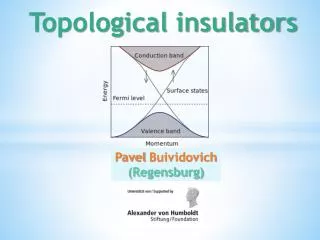
Helicity and large spin-orbit coupling B s v E s • Spin-orbit interaction and surface • E field effectv B = v E in rest frame • spin locked to B • Rashba-like Hamiltonian k E v B k spin aligned with B in rest frame of moving electron Helical, massless Dirac states with opposite chirality on opp. surfaces of crystal Like LH and RH neutrinos in different universes
ARPES results on Bi2Se3 (Hasan group) Xia, Hasan et al. Nature Phys ‘09 Bulk states Large gap ~ 300meV As grown, Fermi level in conduction band Se defect chemistry difficult to control for small DOS
Band bending induced by Gate Voltage (MOSFETs) e e p-type n-type m m b b gap gap e e F F Inversion layer Not applicable to topological insulator gating expt.
Gate tuning of 2-probe resistance in Bi2Se3 m DoS Energy Conductance from surface states? Strong H dependence
Universal Conductance Fluctuations LT Stone, Lee, Fukuyama (PRB 1987) Quantum diffusion Conductance -- sum over Feynman paths H Universal conductance fluctuations (UCF) dG = e2/h in a coherent volume defined by thermal length LT = hD/kT At 1 K, LT ~ 1 mm our xtal For large samples size L, LT “Central-limit theorem” L = 2 mm UCF should be unobservable in a 2-mm crystal!
Into the gap cond. band m valence band target Hor et al., PRB ‘09 Checkelsky et al., PRL ‘09 Solution: Tune m by Ca doping electron doped hole doped Decrease electron density