Topological Insulators & Their Spintronics Application
Topological Insulators & Their Spintronics Application. Xue-sen Wang National University of Singapore phywxs@nus.edu.sg.

Topological Insulators & Their Spintronics Application
E N D
Presentation Transcript
Topological Insulators & Their Spintronics Application Xue-sen Wang National University of Singapore phywxs@nus.edu.sg Topological Insulator: A piece of material that is an insulator (or semiconductor) in its bulk,but supports spin-dependent conductive states at the boundaries due to spin-orbital coupling
Spintronics in Future Information Technology • Spintronics: Manipulation of electron spin for information storage, transmission & processing • Traditional spintronics: e.g. magnetic disk, size limit • Current spintronics: e.g. GMR, TMR, still with a charge current • Ideal Spintronics: Pure spin current & spin accumulation controlled by electric field/voltage, dissipationless • Quantum spin Hall effect (QSHE): an attractive option (S-Q Shen, AAPPS Bulletin 18(5), 29)
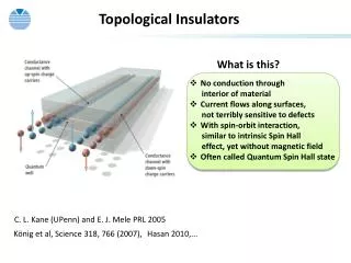
Hall Effect& Spin Hall Effect (SHE) SHE: Separate electrons of different spins without using a magnetic field Spin currentcan be generated & controlled with an electric field or voltage, important tospintronics (From Y.K. Kato, Sci. Am. 2007(10) 88; also see Hirsch, PRL 83, 1834)
Observations of Spin Hall Effect SHE Spin accumulation at edges of GaAs stripe observed by Kerr rotation microscopy (Kato et al., Science 306, 1910) Reverse SHE E Electronic measurement: A spin Hall voltage VSH generated by Reverse-SHE (Valenzuela & Tinkham, Nature 442, 176; Kent, Nature 442, 143)
Spin-dependent scattering Mechanism of SHE: Extrinsic mechanism: Scattering by magnetic field or magnetic impurities Zeeman energy: Stern-Gerlach effect: From relativity, an electron moving in an electric field feels a magnetic field Intrinsic mechanism:
Rashba Effect A moving electric field induces a magnetic field: Intrinsic Rashba spin-orbit coupling: R: small in light atoms (< 1 meV), significantly enhanced in narrow-gap semiconductors containing Bi, Hg… More observable in low-D structures, controllable with electric field V: potential gradient in atom, or at a boundary: 1) Edges of a 2D electron gas 2) Surface or Interface, adjustable with bias voltage
× Boundary states & SHE V = 0 in bulk region if it has inversion symmetry Major contribution to Vstill comes from atomic potential A thin film A stripe of 2DEG Edge Surface Non-zero and oppositeV at two edges (or surfaces) of a 2DEG channel (or a film) Spin-filtered edge (surface) states
Spin-Orbital Coupling in 2DEG or on Surface or: s k ARPES of Bi/Ag(111) (Sinova et al., PRL 92, 126603; Ast et al., PRL 98, 186807)
Quantum Transport in Low-D Systems Quantized conductance through a quantum wire or point contact: Quantum conductance unit: G0 = 2e2/h = 7.75 S Transmitted states (modes)Ntrans, can be changed by gate bias Vg
Edge states & QHE in 2DEG Channel 2DEG in a normal B Skipping Orbits To Edge States Four-terminal Hall resistance: or:
Quantum Hall Effect&Quantum Spin Hall Effect in 2D E Conduction band Valence band k Bulk Insulatorwith Spin-dependent Kramers-pairgaplessedge states Kramers-pair Edge States: elastic backscattering forbidden by time reversal symmetry, robust against weak disorder (Nagaosa, Science 318, 758; Day, Phys. Today 61(1), 19; Kane & Mele, PRL 95, 146802)
M K’ Γ Single-layer graphite: Graphene Graphite Zero bandgap Mass-less (relativistic) fermion Semimetal 3.4 Å Dirac point K 1.42 Å DOS |E|
Spin-filtered edge states: Electrons with opposite spin propagate in opposite direction; jS may be non-dissipative QSHE in Graphene Spin-orbit coupling for edge states: y x A spin current will flow between leads attached to the opposite edges: Quantized SH conductivity: (from Kane & Mele, PRL 95, 226801)
Graphene: a 2D Spin Hall insulator Generate a spin current without dissipation Spin-filtered edge states in graphene are insensitive to disorder: Elastic backscattering is prohibited by time reversal Spin Hall gap in graphene: 2SO ~ 2.4 K (Kane & Mele, PRL 95, 226801; only ~ 0.01 K in Yao et al, PRB 75, 041401) Operation temperature not practical! Existence of other spin Hall insulators with stronger SO interaction?
More attractive materials for Spintronics • Bi, Z = 83; Pb, Z = 82; Hg, Z = 80; strong SOC • Semimetal or narrow-gap semiconductor • Bulk carrier density ~1017 cm-3, low bulk conductivity • Surface carrier density ~1013 cm-2, surface conduction may be dominant • Small effective mass: m* = 0.002m0, ~ 106 cm2/Vs, Fermi velocity vF 106 m/s (comparable with graphene) • 2D & 3D Topological insulators possible • HgTe QW, Bi, Bi1-xSbx , Bi2Se3
QSH Edge States in HgTe QW Inverted Normal 5.5 nm Inverted ? Normal Normal 7.3 nm Critical QW thickness 6.3 nm (König et al., Science 318 (2007) 766)
Lattice Structure of Bi Covalent bond Honeycomb bilayer 3.95 Å a b c 4.545 Å =57.23˚ A C Rhombohedral lattice B Stacking in [111] direction
Bi(111) bilayer: a 2D Spin Hall Insulator [111] Covalent bond 2D bandgap 0.2 eV } 1 Kramerspair of edge states a b c Honeycomb bilayer Spin Hall Conductivity: (Murakami, PRL 97, 236805; Liu et al., PRB 76, 121301)
K M Γ Spin accumulation at edges of Bi(111) bilayer With SOC When EF in middle of Eg Sz + SOC of Bi(111) surface states Splitting ~ 0.1-0.2 eV Sz - No charge current (Koroteev et al., PRL 93, 046403; Liu et al., PRB 76, 121301)
E Conduction band Valence band k Quantum spin Hall Effect in 3D Number of Kramers pairs at each edge/surface must be odd (non-zero Z2 invariant): Strong Topological Insulator (Weak topological insulator: with even number of edge-state pairs) (Kane & Mele, PRL 95, 146802; Fu & Kane, PRB 76, 045302)
Strong Topological Insulator Metallic edge/surface states linear in k meet at an odd number of points in k-space Robust against perturbation (S-c Zhang, APS Physics 1, 6 (2008))
Lattice Structure of Sb & Bi Covalent bond Honeycomb bilayer Sb: 3.76 Å Bi: 3.95 Å a Sb: 4.31 Å Bi: 4.545 Å b c = 57.1 (Sb) = 57.23° (Bi) A C Rhombohedral lattice: A distorted simple cubic (SC) or FCC lattice B
Electronic Structure of Bi & Sb Ls Band overlap 38 meV L EF= 26.7 meV T 13.8 meV La (for Sb: at H, 177 meV overlap with inverted La) Semimetal Low carrier density (~1017 cm-3) Small effective mass High carrier mobility (~ 105 cm2/Vs) Long F, ~ 120 Å
E H T Inversion of L bands La La Ls 30 meV La Ls Ls H T x (%) 0 4 7 9 17 22 Semiconductoror Topological Insulator Energy Bands of Bi1-xSbx @ x ~ 4%: Dirac Fermions in 3+1 D
Bi1-xSbx: Topological Insulator (x ~ 7-10%) m* ~ 0.002me 2D quantum spin Hall phase 1D edge states 3D quantum spin Hall phase 2D surface states (Hsieh et al., Nature 452, 970; Teo et al., PRB 78, 045426)
Effect of SOC on Bi bulk band near EF = 13.7 meV 3D Dirac point at L (Hsieh et al., Nature 452, 970 (Suppl. Info.))
Surface States on Different Bi1-xSbx Surfaces “Strong” Topological Insulator Surface Fermi arc encloses 1 or 3 Dirac points on all surfaces (111) & (110) surfaces commonly observable Surface time-reversal-invariant momentum (TRIM) enclosed by an odd number of electron or hole pockets (from Teo, Fu & Kane, PRB 78, 045426)
Bi(111) Surface ARPES measurement of surface states EF mapping Spin direction of states at EF (Hofmann, Prog. Surf. Sci. 81, 191; Ast & Hochst, PRL 87, 177602)
ARPES & computed of surface states Bi(110) Surfaces EF mapping & spin directions (Hofmann, Prog. Surf. Sci. 81, 191; Pascual et al., PRL 93, 196802)
Bi & Sb Nanostructures Grown on Inert Substrates • HOPG or MoS2 cleaved in air, ~ 5 hours degas at 300-550C in UHV • Sb & Bi from thermal evaporators • Nearly free-standing structures grow on aninert surface • STM imaging at RT UHV STM system
(100 nm)2 3D, 2D & 1D Sb Nanostructures on HOPG 1D, h ~ 23 nm 3D, h ~ 60 nm 2D, h ~ 3.5 nm (111)-oriented 2D islands Lateral period: a = 4.170.12 Å (1000 nm)2 Sb4, F = 4 Å/min, 12 Å deposited at RT. 3D, 2D & 1D islands formed at early stage Bulk Sb: a = 4.31 Å (10 nm)2
1D & 2D Bi Nanostructures on HOPG (0.6 m)2 1D nanobelts (1 m)2 2D islands, height ~ 1 nm (111) oriented Bi(111) bilayer spacing: 3.95 Å
Bi Nanobelts: (110) oriented (200 nm)2 Narrow belts on top of wide belt Narrow belt h ~ 8 Å (2 m)2 Height ~ 1-10 nm Width ~ 25-70 nm Belt surface with rectangular lattice: 4.34 Å × 4.67 Å Bulk Bi(110): 4.55 Å × 4.75 Å Layer spacing: 3.28 Å (9 nm)2
Aligned Bi Nanobelt on Low-symmetry Surface Bi(110) nanobelts on Bi/Ag(111) Bi wetting layer on Ag(111): with a 2D rectangular lattice Aligned Bi nanobelts on Si(111)-41:In single-domain terrace observed in Surface Physics Lab, Inst. of Physics, CAS, Beijing (300 nm)2
Self-Assembly of Sb & Bi Nanobelts Deposited atoms Growth direction Dangling bonds (111) top surface of Bi nanobelt Inert sidewall Removal of dangling bonds on Bi(110) by “puckered-layer” atomic reconfiguration (Nagao et al. PRL 2004)
Transformation of Bi(110) to Bi(111) (1 m)2 (1 m)2 After 10 min 100C anneal h ~ 5 – 9 nm After 10 min 130C anneal h ~ 5 – 10 nm
Topological Insulators at Room Temperature Surface states on (111) Bi2Se3: Eg 0.3 eV Sb2Te3: Eg 0.1 eV (H. Zhang et al., Nature Physics 5 (2009) 438)
Magneto-Electric Effects in Topological Insulators Normal insulator: Additional action term: where All time reversal invariant insulators can be divided into two classes: Topological insulator: θ = π Normal insulator: θ = 0; (Qi, Hughes and Zhang, PRB 78, 195424)
Topological Magneto-Electric (TME) Effect P3 = θ/2π A charge near TI induces an image magnetic monopole: g (Qi, Hughes and Zhang, PRB 78, 195424; Qi et al, arXiv:0811.1303)
Summary • Topological insulators possess novel properties with potential spintronic applications due to QSHE • HgTe QW, Bi(111) monolayer, Bi1-xSbx alloy, Bi2Se3 and Sb2Te3 are possible topological insulators • Bi(111) bilayer/film similar to graphene/graphite • Ultrathin (2-6 bilayers) Bi(111) and Bi(110) nanobelts can be obtained on inert substrates (e.g. graphite and MoS2) • Bi & Sb nanostructures can be fabricated at much less demanding conditions than for graphene. Certain growth controls have been accomplished
Further Studies • Fabrication of Bi1-xSbx (x ~ 10%) thin films and nanostructures, effect of inhomogeneity • Electronic & spintronic transport measurements, TME effect: contact, patterning and processing • Controlled growth of Bi & BiSb structures on Si-based substrates • Other topological materials, e.g. Bi2Se3, Sb2Te3
Universal Intrinsic Spin Hall Effect in 2DEG s Spin current is polarized in z direction, with spin Hall conductivity p Still need charge current (Sinova et al., PRL 92, 126603)
V1 V2 U Phases of Honeycomb Lattice with Repulsive Interactions QSE phase more likely in bilayer lattice of dipolar atoms with V2 > U, V1 (Raghu et al., PRL 100, 156401)
y D C B x A Lattice distortion across 90-elbow of Bi nanobelt Variation of X-period D:ax = 4.88 Å C:ax = 4.73 Å B:ax = 4.49 Å A:ax = 4.47 Å Reverse variation of Y-period On bulk Bi(110): 4.55 Å × 4.75 Å
2 bilayer (~ 6.6 Å) Bi(110) growth On Ag(111) with a Bi wetting layer
Semimetal-to-Semiconductor transition in Bi nanowires (Lin et al., PRB 62, 4610)
Bi(111) Ultrathin Films 1 bilayer: Semiconducting 2 – 3 bilayer films: Semimetallic electron hole With SOC (Koroteev et al., PRB 77, 045428)
Bi(110): bilayer pairing Remove dangling bonds on Bi(011) by “puckered-layer” pairing reconfiguration (Nagao et al. PRL 2004) >10% in vacuum (Koroteev et al., PRB 77, 045428)